Alkaline earth metal-containing cleaning solution for cleaning semiconductor element, and method for cleaning semiconductor element using same

a technology of alkaline earth metal and cleaning solution, which is applied in the direction of detergent compounding agent, inorganic non-surface active detergent composition, instruments, etc., can solve the problems of reducing the quality of cleaning solution, and accelerating the miniaturization of design rules, etc., to achieve high quality, reduce the damage, and reduce the effect of aging

Active Publication Date: 2017-11-23
MITSUBISHI GAS CHEM CO INC
View PDF2 Cites 7 Cited by
  • Summary
  • Abstract
  • Description
  • Claims
  • Application Information

AI Technical Summary

Benefits of technology

[0056]By employing the cleaning solution of the present invention and the cleaning method using the same, it is possible to suppress damage to at least a low-k film and at least one material selected from between a titanium-containing material and a tungsten-containing material and selectively remove a dry etching residue and a photoresist on a surface of a product to be treated in the process for manufacturing a semiconductor element, and it is possible to produce a semiconductor element having high precision and high quality with a high yield.

Problems solved by technology

Recently, the miniaturization of design rules has been accelerated, and the limit of high-speed arithmetic processing has been gradually controlled by signal transmission delay.
Patterns of 0.2 μm or less have problems in which, for example, the aspect ratio of a pattern of a photoresist having a film thickness of 1 μm (the ratio obtained by dividing the film thickness of the photoresist by the line width of the photoresist) is too large, resulting in collapse of the pattern.
Since a hard mask, a low-k film, a tungsten-containing material and copper or a copper alloy are exposed in the process of removing a dry etching residue and a photoresist in this way, when a dry etching residue and a photoresist are removed with oxygen plasma, the hard mask, the low-k film, the tungsten-containing material and the copper or copper alloy are damaged due to exposure to oxygen plasma or the like, resulting in significant deterioration of electrical characteristics and problems in production processes after that.
The strong alkali-based cleaning solution may remove a residue, but its removability of the dry etching residue and the photoresist is inferior to that of the oxidant-containing cleaning solution.
Meanwhile, the oxidant-containing cleaning solution has excellent removability of the dry etching residue and the photoresist, but when it is brought into contact with a material containing titanium or tungsten, the material containing titanium or tungsten is significantly damaged.
When using this cleaning solution, it is possible to remove a residue while suppressing damage to a low-k film, but damage to a titanium-containing material cannot be suppressed.
When using this cleaning solution, it is possible to suppress damage to a titanium-containing material, but a residue cannot be removed, and damage to a low-k film cannot be suppressed.
When using this cleaning solution, it is possible to suppress damage to a tungsten-containing material, but a residue cannot be removed, and damage to a low-k film cannot be suppressed.
When using this cleaning solution, it is possible to suppress damage to a low-k film while removing a residue, but damage to a tungsten-containing material cannot be suppressed.
When using this cleaning solution, it is possible to suppress damage to a tungsten-containing material, but a residue cannot be removed, and damage to a low-k film cannot be suppressed.
When using this cleaning solution, it is possible to remove a residue, but damage to a tungsten-containing material and a low-k film cannot be suppressed.
When using this cleaning solution, it is possible to suppress damage to a tungsten-containing material, but a residue cannot be removed, and damage to a low-k film cannot be suppressed.
When using this cleaning solution, it is possible to suppress damage to a low-k film, but a residue cannot be removed, and damage to a tungsten-containing material cannot be suppressed.
When using this cleaning solution, it is possible to suppress damage to a tungsten-containing material, but a residue cannot be removed, and damage to a low-k film cannot be suppressed.
When using this cleaning solution, it is possible to suppress damage to a tungsten-containing material, but a residue cannot be removed, and damage to copper or a copper alloy, a low-k film and a titanium-containing material cannot be suppressed.
When using this cleaning solution, it is possible to suppress damage to a tungsten-containing material, copper or a copper alloy and a titanium-containing material, but a residue cannot be removed, and damage to a low-k film cannot be suppressed.
When using this cleaning solution, it is possible to suppress damage to a tungsten-containing material and a titanium-containing material, but a residue cannot be removed, and damage to copper or a copper alloy and a low-k film cannot be suppressed.
When using the cleaning solution described in Patent Document 22, it is impossible to remove a dry etching residue, and it is impossible to suppress damage to a tungsten-containing material and a low-k film.
However, when using the cleaning solution described in Patent Document 23, it is impossible to remove a dry etching residue, and it is impossible to suppress damage to a titanium-containing material, a tungsten-containing material and copper.

Method used


Image

  • Alkaline earth metal-containing cleaning solution for cleaning semiconductor element, and method for cleaning semiconductor element using same
  • Alkaline earth metal-containing cleaning solution for cleaning semiconductor element, and method for cleaning semiconductor element using same
  • Alkaline earth metal-containing cleaning solution for cleaning semiconductor element, and method for cleaning semiconductor element using same

Examples


examples

[0096]Hereinafter, the present invention will be described in more detail based on Examples and Comparative Examples, but the present invention is not limited by the Examples.

SEM Observation:

[0097]Observation of conditions before and after the cleaning / removal treatment of the semiconductor element was carried out using the below-described SEM (scanning electron microscope) apparatus (100,000 x).

[0098]Measurement apparatus: ultra-high resolution field-emission scanning electron microscope SU9000 manufactured by Hitachi High-Technologies Corporation

Judgment:

[0099]The judgment after cleaning / removal was made after SEM observation based on the below-described criteria.

I. Removal State of Dry Etching Residue

[0100]E: The dry etching residue was completely removed.

[0101]G: The dry etching residue was almost removed.

[0102]P: The dry etching residue was insufficiently removed.

[0103]E and G are regarded as acceptable.

II. Damage to Titanium-Containing Material

[0104]E: The titanium-containing ...

examples 1-22

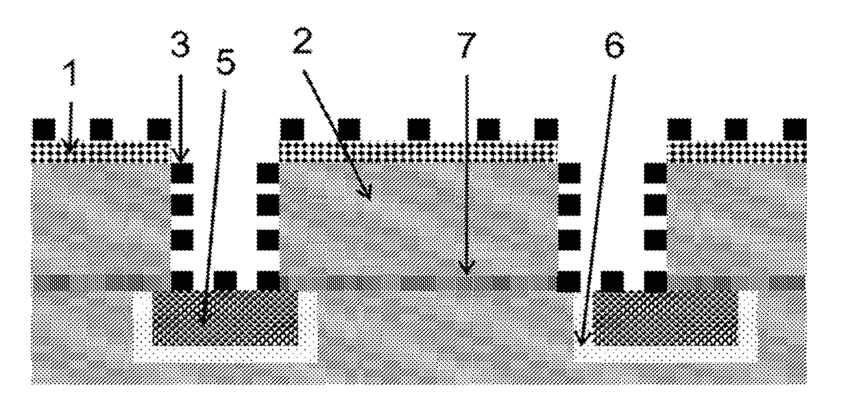
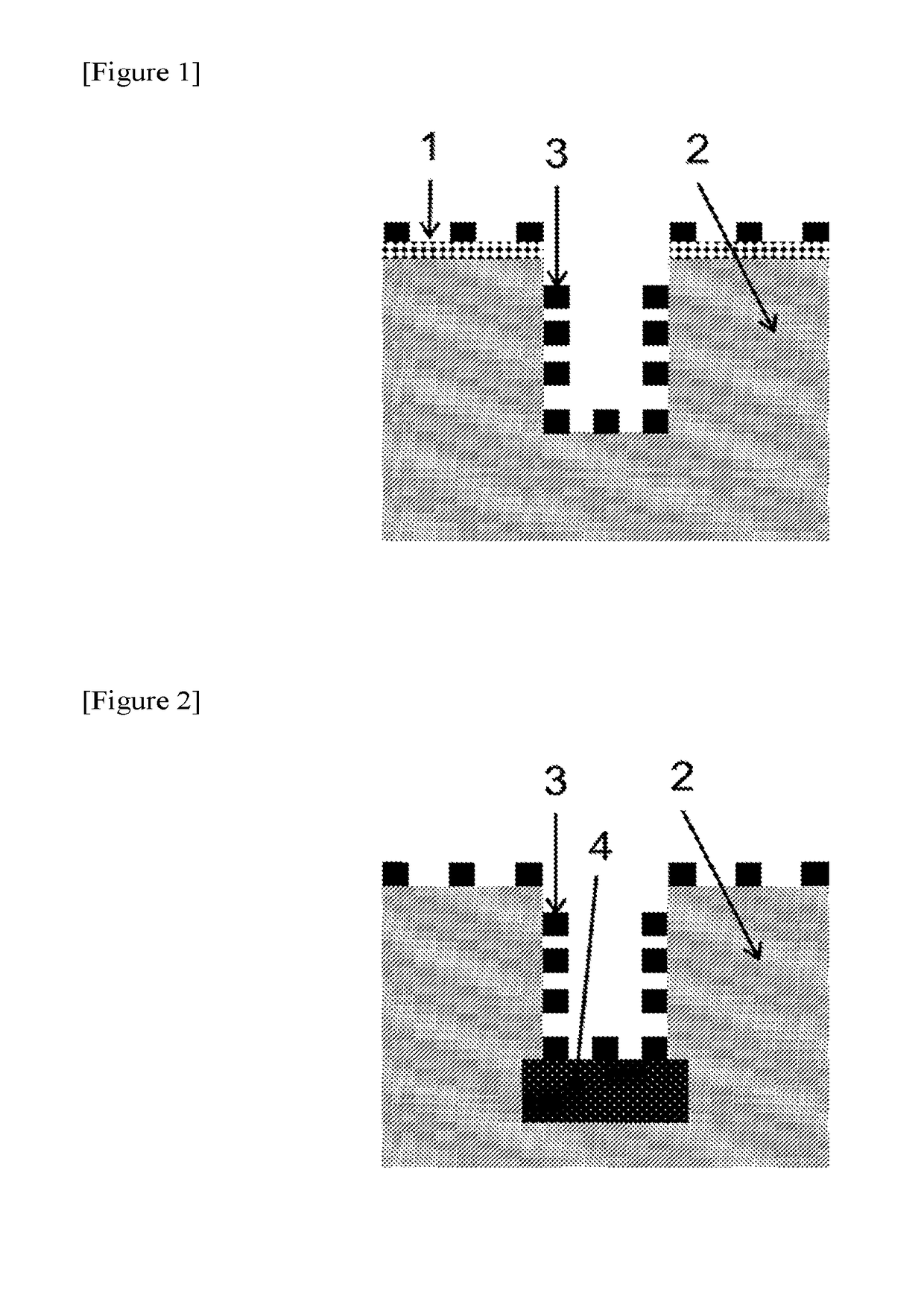
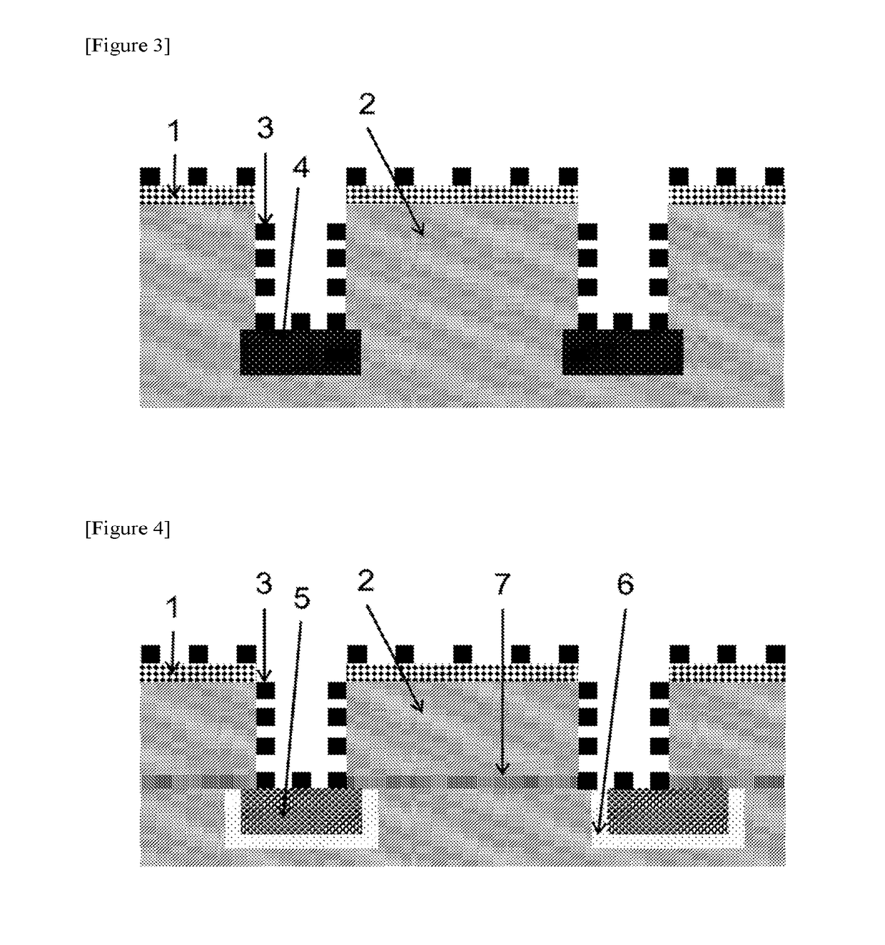
[0127]The semiconductor element shown in FIG. 1 was cleaned with the cleaning solution of the present invention shown in Table 1. The results are shown in Table 2. It is understood that in Examples 1-22, damage to the titanium-containing material 1 and the low-k film 2 was prevented while the dry etching residue 3 was completely removed.

examples 23-41

[0128]The semiconductor element shown in FIG. 2 was cleaned with the cleaning solution of the present invention shown in Table 1. The results are shown in Table 3. It is understood that in Examples 23-41, damage to the tungsten-containing material 4 and the low-k film 2 was prevented while the dry etching residue 3 was completely removed.


PUM

PropertyMeasurementUnit
dielectric constantaaaaaaaaaa
thicknessaaaaaaaaaa
thicknessaaaaaaaaaa

Abstract

According to the present invention, it is possible to provide a cleaning solution which removes a dry etching residue and photoresist on a surface of a semiconductor element having a low dielectric constant film (a low-k film) and at least one material selected from between a material that contains 10 atom % or more of titanium and a material that contains 10 atom % or more of tungsten, wherein the cleaning solution contains: 0.002-50 mass % of at least one type of oxidizing agent selected from among a peroxide, perchloric acid, and a perchlorate salt; 0.000001-5 mass % of an alkaline earth metal compound; and water.

Description

TECHNICAL FIELD[0001]The present invention relates to a cleaning solution, which suppresses damage to at least a low-dielectric constant interlayer dielectric film and at least one material selected from a titanium-containing material and a tungsten-containing material and removes a dry etching residue and a photoresist on a surface of a product to be treated in the process for manufacturing a semiconductor element, and a cleaning method using the same.BACKGROUND ART[0002]The production of a highly integrated semiconductor element generally has a series of processes as follows: a conductive thin film such as a metal film as a conductive wiring material and an interlayer dielectric film for insulation between conductive thin films are formed on an element such as a silicon wafer; after that, a photoresist is uniformly applied to the surface thereof to provide a photosensitive layer, and this is subjected to the selective exposure / development treatment to form a desired photoresist pa...

Claims


Application Information

Patent Timeline
Patent Type & Authority Applications(United States)
IPC IPC(8): C11D7/10H01L21/02C11D7/26H01L21/311H01L21/768
CPCC11D7/105C11D7/26H01L21/76814H01L21/31116H01L21/31144H01L21/02063C11D7/02C11D17/08H01L21/31133G03F7/423C11D11/0047C11D3/046H01L21/02052
Inventor OIE, TOSHIYUKISHIMADA, KENJI
Owner MITSUBISHI GAS CHEM CO INC
Why Eureka
Try Eureka