Resist composition and patterning process

a composition and patterning technology, applied in the field of resist composition, can solve the problems of reducing the resolution and focus margin of hole and trench pattern, lwr degradation, serious problems, etc., and achieves the effects of high sensitivity, high atomic weight, and suppressing acid diffusion

Active Publication Date: 2017-12-28
SHIN ETSU CHEM IND CO LTD
View PDF1 Cites 17 Cited by
  • Summary
  • Abstract
  • Description
  • Claims
  • Application Information

AI Technical Summary

Benefits of technology

[0020]A resist material containing a sulfonium or iodonium salt of iodized benzoyloxy-containing fluorinated sulfonic acid has the advantage that the salt is highly effective for suppressing acid diffusion because of the large atomic weight of iodine. Since iodine is highly absorptive to EUV of wavelength 13.5 nm, it generates secondary electrons during exposure, contributing to a higher sensitivity. Thus a resist material having a high sensitivity, low LWR and improved CDU may be designed.

Problems solved by technology

In the case of positive resist film, a lowering of light contrast leads to reductions of resolution and focus margin of hole and trench patterns.
A film thickness reduction to comply with the progress of size reduction causes a degradation of LWR, which becomes a serious problem.

Method used


Image

  • Resist composition and patterning process
  • Resist composition and patterning process
  • Resist composition and patterning process

Examples


example

[0107]Examples of the invention are given below by way of illustration and not by way of limitation. The abbreviation “pbw” is parts by weight.

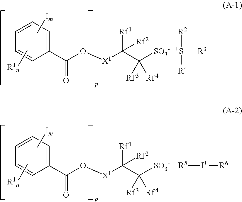
[0108]Sulfonium or iodonium salts, designated PAG1 to PAG29, used in resist compositions are identified below. PAG1 to PAG29 were synthesized by ion exchange between an iodized benzoyloxy-containing fluorinated sulfonic acid providing the anion shown below and a sulfonium or iodonium chloride providing the cation shown below.

Synthesis Example: Synthesis of Base Polymers (Polymers 1 to 4)

[0109]Base polymers were prepared by combining suitable monomers, effecting copolymerization reaction thereof in tetrahydrofuran (THF) solvent, pouring the reaction solution into methanol for crystallization, repeatedly washing with hexane, isolation, and drying. The resulting polymers, designated Polymers 1 to 4, were analyzed for composition by 1H-NMR spectroscopy, and for Mw and Mw / Mn by GPC versus polystyrene standards using THF solvent.

examples 1-1 to 1-12

and Comparative Examples 1-1 to 1-4

[0119]On a substrate (silicon wafer), a spin-on carbon film ODL-102 (Shin-Etsu Chemical Co., Ltd., carbon content 80 wt %) was deposited to a thickness of 200 nm and a silicon-containing spin-on hard mask SHB-A940 (Shin-Etsu Chemical Co., Ltd., silicon content 43 wt %) was deposited thereon to a thickness of 35 nm. On this substrate for trilayer process, each of the resist compositions in Table 1 was spin coated, then baked on a hot plate at 100° C. for 60 seconds to form a resist film of 80 nm thick.

[0120]Using an ArF excimer laser scanner NSR-S610C (Nikon Corp., NA 1.30, σ 0.98 / 0.78, 35° cross-pole illumination, azimuthally polarized illumination), the resist film was exposed through a 6% halftone phase shift mask bearing a pattern having a line of 50 inn and a pitch of 100 nm (on-wafer size). The resist film was baked (PEB) at the temperature shown in Table 1 for 60 seconds. Thereafter, the resist film was developed in n-butyl acetate for 30 sec...

examples 2-1 to 2-19

and Comparative Example 2-1

[0122]The resist composition in Table 2 was spin coated on a silicon substrate having a 20-nm coating of silicon-containing spin-on hard mask SHB-A940 (Shin-Etsu Chemical Co., Ltd., Si content 43 wt %) and prebaked on a hot plate at 105° C. for 60 seconds to form a resist film of 60 nm thick. Using an EUV scanner NXE3300 (ASML, NA 0.33, σ 0.9 / 0.6, quadrupole illumination), the resist film was exposed to EUV through a mask bearing a hole pattern at a pitch 46 nm (on-wafer size) and +20% bias. The resist film was baked (PEB) on a hot plate at the temperature shown in Table 2 for 60 seconds and developed in a 2.38 wt % TMAH aqueous solution for 30 seconds to form a hole pattern having a size of 23 nm.

[0123]The resist pattern was evaluated. The exposure dose that provides a hole pattern having a size of 23 nm is reported as sensitivity. The size of 50 holes was measured under CD-SEM (CG-5000, Hitachi High-Technologies Corp.), from which a size variation (36) w...


PUM

PropertyMeasurementUnit
wavelengthaaaaaaaaaa
of wavelengthaaaaaaaaaa

Abstract

A resist composition comprising a base polymer and a sulfonium or iodonium salt of iodized benzoyloxy-containing fluorinated sulfonic acid offers a high sensitivity and minimal LWR or improved CDU independent of whether it is of positive or negative tone.

Description

CROSS-REFERENCE TO RELATED APPLICATION[0001]This non-provisional application claims priority under 35 U.S.C. §119(a) on Patent Application No. 2016-127556 filed in Japan on Jun. 28, 2016, the entire contents of which are hereby incorporated by reference.TECHNICAL FIELD[0002]This invention relates to a resist composition comprising a sulfonium or iodonium salt of iodized benzoyloxy-containing fluorinated sulfonic acid and a pattern forming process.BACKGROUND ART[0003]To meet the demand for higher integration density and operating speed of LSIs, the effort to reduce the pattern rule is in rapid progress. The wide-spreading flash memory market and the demand for increased storage capacities drive forward the miniaturization technology. As the advanced miniaturization technology, manufacturing of microelectronic devices at the 65-nm node by the ArF lithography has been implemented in a mass scale. Manufacturing of 45-nm node devices by the next generation ArF immersion lithography is ap...

Claims


Application Information

Patent Timeline
Patent Type & Authority Applications(United States)
IPC IPC(8): C08F220/30G03F7/039C09D133/14H01S3/00C08F220/38
CPCC08F220/30H01S3/0007C08F220/38C09D133/14G03F7/0395G03F7/0045G03F7/0046G03F7/0382G03F7/0397C08F220/22C08F220/283C08F220/1807C08F220/1809C08F220/382C08F220/301C08F220/1818C08F220/20C08F220/24G03F7/039G03F7/038G03F7/004G03F7/26C07C381/12C07C25/18
Inventor HATAKEYAMA, JUNOHASHI, MASAKIFUJIWARA, TAKAYUKIFUKUSHIMA, MASAHIROHONDA, KAZUYA
Owner SHIN ETSU CHEM IND CO LTD
Why Eureka
Try Eureka