Integrated method for wafer outgassing reduction

a technology of integrated circuits and wafers, applied in the direction of coatings, vacuum evaporation coatings, chemical vapor deposition coatings, etc., can solve the problems of affecting the crystallinity, and affecting the temperature pyrometer reading

Inactive Publication Date: 2018-03-15
APPLIED MATERIALS INC
View PDF3 Cites 91 Cited by
  • Summary
  • Abstract
  • Description
  • Claims
  • Application Information

AI Technical Summary

Benefits of technology

[0009]In yet another implementation, the method includes transferring a substrate into a substrate processing region of a plasma chamber, wherein the substrate has an exposed silicon-containing surface, removing oxides from the exposed silicon-containing surface by use of a first plasma etch process, comprising flowing a fluorine-containing precursor and an inert gas into the substrate processing region while applying a plasma power to form fluorine ions and inert gas ions, and etching the silicon-containing surface with the fluorine ions and the hydrogen-containing ions while applying a bias to the substrate to form an etched silicon-containing surface, transferring the substrate from the plasma chamber to an epitaxial deposition chamber, forming an epitaxial layer comprising arsenic on the exposed surface of the substr...

Problems solved by technology

Ion implantation of chemical impurities disrupts the crystallinity of the semiconductor substrate over the range of the implant.
However, the implanted dopants will not come to rest on electrically active sites in the substrate.
This deposition may interfere with temperature pyrometer readings and with the radiation distribution fields on the substrate, which in turn affects the temperature at which the substrate is anneale...

Method used


Image

  • Integrated method for wafer outgassing reduction
  • Integrated method for wafer outgassing reduction
  • Integrated method for wafer outgassing reduction

Examples


Embodiment Construction

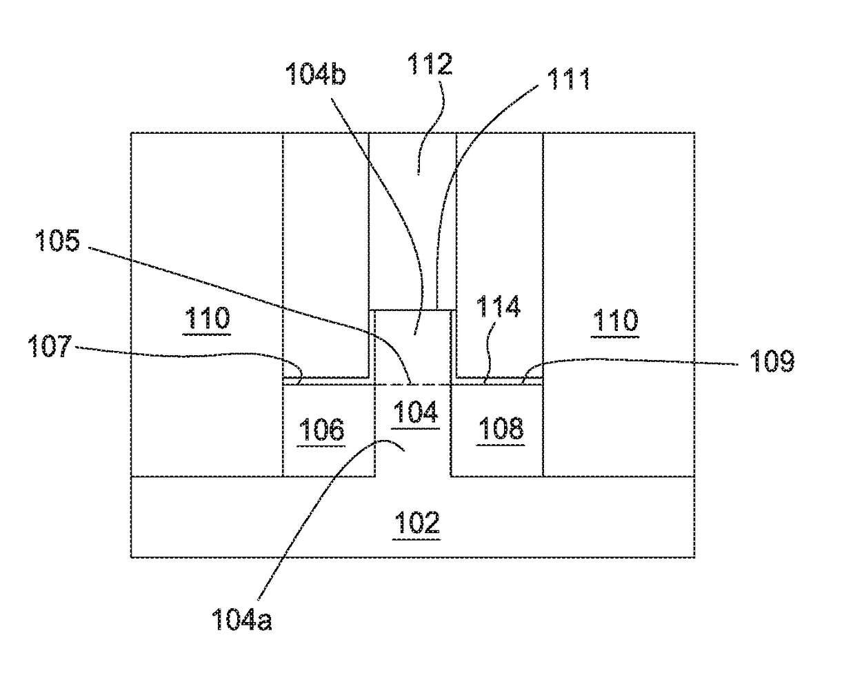
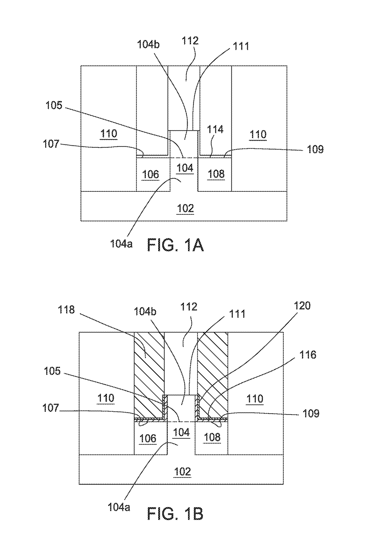
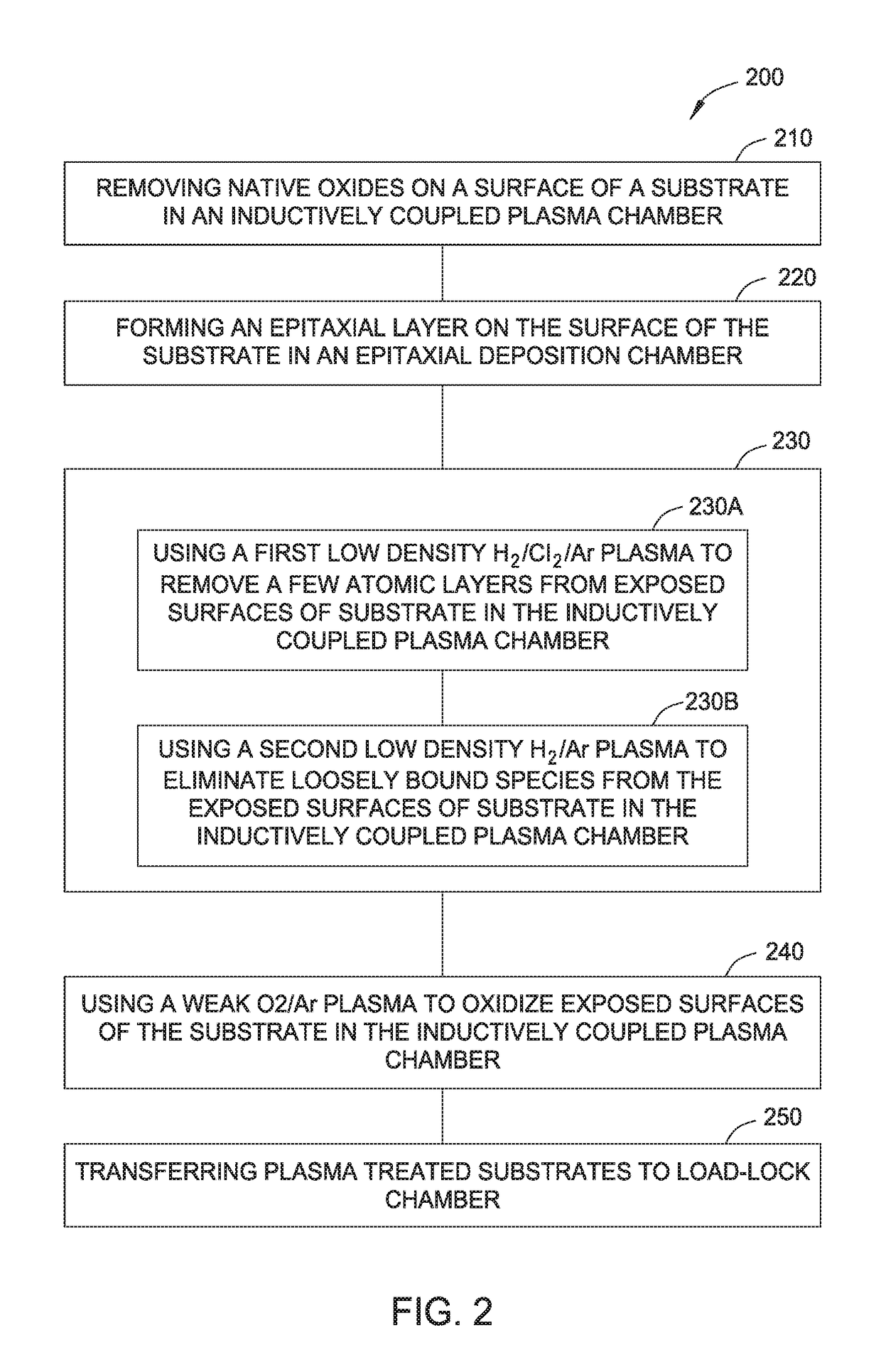
[0016]FIGS. 1A and 1B depict a cross-sectional view of a semiconductor structure 100 that may be processed utilizing the method depicted in FIG. 2. The semiconductor structure 100 forms a portion of a circuit device. In one implementation shown in FIG. 1A, the semiconductor structure 100 includes a substrate 102 and a plurality of fin structures 104 (only one is shown) extending upwardly from the substrate 102. A source region 106 and a drain region 108 are formed approximately adjacent to the fin structure 104 on opposite sides of the fin structure 104. The fin structure 104, the source region 106, and the drain region 108 are surrounded by a dielectric material 110. For PMOS transistor devices, the source region 106 and the drain region 108 are typically doped with P-type impurities, such as boron. For NMOS transistor devices, the source region 106 and the drain region 108 are typically doped with N-type impurities such as arsenic or phosphorous.

[0017]The substrate 102 may be a ma...


PUM

PropertyMeasurementUnit
Fractionaaaaaaaaaa
Pressureaaaaaaaaaa
Pressureaaaaaaaaaa

Abstract

Implementations disclosed herein relate to methods for controlling substrate outgassing. In one implementation, the method includes removing oxides from an exposed surface of a substrate in an inductively coupled plasma chamber, forming an epitaxial layer on the exposed surface of the substrate in an epitaxial deposition chamber, and performing an outgassing control of the substrate by subjecting the substrate to a first plasma formed from a first etch precursor in the inductively coupled plasma chamber at a first chamber pressure, wherein the first etch precursor comprises a hydrogen-containing precursor, a chlorine-containing precursor, and an inert gas, and subjecting the substrate to a second plasma formed from a second etch precursor in the inductively coupled plasma chamber at a second chamber pressure that is higher than the first chamber pressure, wherein the second etch precursor comprises a hydrogen-containing precursor and an inert gas.

Description

CROSS-REFERENCE TO RELATED APPLICATIONS[0001]This application claims priority to U.S. provisional patent application Ser. No. 62 / 395,212, filed Sep. 15, 2016, which is herein incorporated by reference.BACKGROUNDField[0002]Implementations of the present disclosure generally relate to the fabrication of integrated circuits. More specifically, implementations disclosed herein relate to methods for controlling substrate outgassing.Description of the Related Art[0003]Ion implementation is a method for the introduction of chemical impurities in semiconductor substrates to form the p-n junctions necessary for field effect or bipolar transistor fabrication. Such impurities include P-type dopants, such as boron, aluminum, gallium, beryllium, magnesium, and zinc, and N-type dopants such as phosphorus, arsenic, antimony, bismuth, selenium, and tellurium. Ion implantation of chemical impurities disrupts the crystallinity of the semiconductor substrate over the range of the implant. At low energ...

Claims


Application Information

Patent Timeline
IPC IPC(8): H01L21/02H01L29/78H01L29/08
CPCH01L21/02664H01L21/02661H01L29/0847H01L21/02236H01L29/785H01L21/0262C23C16/0245C23C16/24C23C16/56H01L29/66795H01L21/02057H01L21/02063H01L21/02238H01L21/02252C23C14/021C23C14/022C23C14/5873H01L21/02293H01L21/02315H01L21/0234H01L21/02634H01L21/76855
Inventor YAN, CHUNBAO, XINYUCHUNG, HUACHU, SCHUBERT S.
Owner APPLIED MATERIALS INC
Why Eureka
Try Eureka