Photoluminescent polarizers and electronic devices including the same

Active Publication Date: 2018-07-05
SAMSUNG ELECTRONICS CO LTD +1
View PDF2 Cites 4 Cited by
  • Summary
  • Abstract
  • Description
  • Claims
  • Application Information

AI Technical Summary

Benefits of technology

[0050]Embodiments of the photoluminescent polarizer may include a high quality sharp edge V-grooves and a nanocrystal composite disposed on a surface thereof and may emit polarized light from a front surface thereof. Accordingly, the photoluminescent polarizer of the

Problems solved by technology

Therefore, the optical efficie

Method used


Image

  • Photoluminescent polarizers and electronic devices including the same
  • Photoluminescent polarizers and electronic devices including the same
  • Photoluminescent polarizers and electronic devices including the same

Examples


Example

Reference Example 1: Production of CdTe QD Nanocrystal

[0176]4.59 grams (g) of Cd(ClO4)2 is dissolved in 0.2 liter (L) of MILLI-Q® water (ultrapure water) to prepare a solution (Step 1), with which 0.3 L of a solution including MILLI-Q® water and 1.31 g of thioglycolic acid (“TGA”) are mixed in a first flask (Step 2) to form 0.5 L of a mixed solution. Then, by the addition of NaOH thereto with vigorous stirring, the resulting mixture having a pH of 12 is prepared as a Cd-containing solution. In a glove box, 0.8 g of Al2Te3 is placed in a second flask while argon gas is flowed thereinto. A sulfuric acid solution is prepared by mixing 10 mL of 0.5 M H2SO4 with 15 mL of MILLI-Q® water. The second flask is connected to the first flask and the sulfuric acid solution is added to the Al2Te3 and the argon gas is used as a carrier to provide H2Te gas. After 30 minutes, the Al2Te3 line is disconnected and the reaction system is heated to 100° C. for the solution to boil, thereby quantum dots a...

Example

Example 1: Production of Corrugated PDMS Structure (Replica)

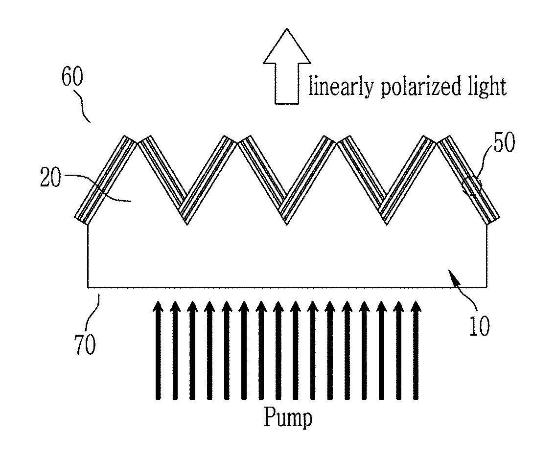
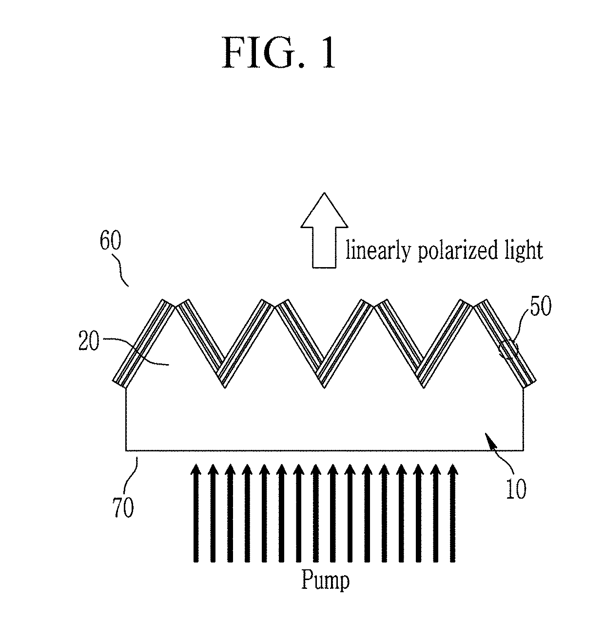
[0177]A corrugated PDMS structure (replica) is obtained according to the method illustrated in FIGS. 6A to 6F.

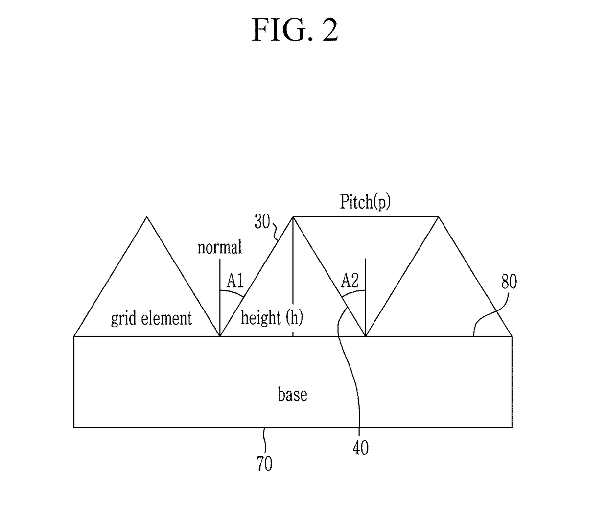
[0178]On a silicon substrate, a 200 nm thick PMMA bilayer (495 K molecular weight at the bottom and 950 K molecular weight at the top) is coated using spin coating. A 50 nm chromium layer is deposited via electron beam deposition. The PMMA layer having the chromium layer thereon is lifted off by using dichloroethane and the shallow deep reactive etching is conducted to pattern the silicon substrate. For the wet etching, IPA is added to KOH etch recipe in order to decrease an etch rate. The remaining chromium layer plays a role of a protective mask layer while an anisotropic KOH etching is conducted at a temperature of 40° C. at an etch rate of 70 nm / min to obtain a mold having a corrugated surface. In the corrugated surface, the first lateral faces and the second lateral faces are angled toward each other to form a ...

Example

Example 2: Production of a Photoluminescent Unit Stack on the Corrugated PDMS Replica

[0181]According to the method illustrated in FIGS. 6A to 6F, a PDMS replica having a corrugated surface is prepared as below.

[0182]On the PDMS replica is formed a 15 nm thick gold (Au) layer via electron beam deposition. Each of a PDDA solution and a PSS solution is prepared by dissolving poly(diallyldimethylammonium) chloride (PDDA) or polystyrene sulfonate (PSS), respectively. Each of the PDDA solution and the PSS solution is coated on the Au layer and the solvent is removed therefrom to form a spacer including the PDDA / PSS bilayer. A 15 nm thick gold (Au) layer is deposited on the spacer and then four PDDA / PSS bilayers are formed on the Au layer via a spin or dip coating. Then, a CdTe QD aqueous solution prepared in Reference Example 1 is prepared on the spacer and the solvent is removed to form a quantum dot monolayer. Another four PDDA / PSS bilayers are formed on the quantum dot monolayer to obt...


PUM

PropertyMeasurementUnit
Fractionaaaaaaaaaa
Thicknessaaaaaaaaaa
Thicknessaaaaaaaaaa

Abstract

A photoluminescent polarizer including: a base having a first surface, a second surface opposite to the first surface, and a plurality of grid elements disposed on the first surface; wherein a grid element includes a first lateral face, a second lateral face, and at least one photoluminescent unit stack disposed on at least one of the first lateral face and the second lateral face, wherein the first lateral face is angled away from a line perpendicular to the first surface of the base and the second lateral face angled toward the first lateral face and away from the line, wherein the photoluminescent unit stack is disposed on at least one of the first lateral face and/or to the second lateral face, wherein the photoluminescent unit stack comprises a light emitting film and a metal film, the metal film disposed on a surface of the light emitting film.

Description

CROSS-REFERENCE TO RELATED APPLICATION[0001]This application claims priority to Korean Patent Application No. 10-2017-0001578 filed on Jan. 4, 2017, and all the benefits accruing therefrom under 35 U.S.C. § 119, the content of which is incorporated herein in its entirety by reference.BACKGROUND1. Field[0002]Embodiments of a photoluminescent polarizer and an electronic device including the same are disclosed.2. Description of the Related Art[0003]A panel display such as a Liquid Crystal Display (“LCD”) device is a non-emissive type of display that may utilize an external light source to display information. A backlight unit disposed at the back of the display panel may emit non-polarized light, which passes through a polarizer, is thereby converted to polarized light, and then passes through a panel including a liquid crystal layer, a color filter, and / or another polarizer, and finally provides image information to a final user. The light provided by the backlight unit including a li...

Claims


Application Information

Patent Timeline
IPC IPC(8): G02F1/1335G02F1/1337
CPCG02F1/133617G02F1/133528G02F1/13362G02F1/133711H01L33/58G02F2001/133614G02F1/133536G02F2202/36G02F1/133548G02F1/133614H10K50/86G02B5/3058G02B5/008C09K11/08H01L21/02601H01L29/0669G02B6/1226H10K50/00
Inventor JUN, SHIN AEDEMIR, HILMI VOLKANJANG, EUN JOOGUZELTURK, BURAKGUNGOR, KIYANCERDEM, ONUR
Owner SAMSUNG ELECTRONICS CO LTD
Why Eureka
Try Eureka