
High-Speed MOSFET and IGBT Gate Driver

a gate driver and high-speed technology, applied in the field of high-speed gate drivers, can solve the problems of increasing the cost of another part of the circuit, reducing the cost in certain respects, and often remaining undetected high cos

Inactive Publication Date: 2018-08-02
LITTELFUSE INC
View PDF1 Cites 1 Cited by
  • Summary
  • Abstract
  • Description
  • Claims
  • Application Information

AI Technical Summary

Benefits of technology

The patent text describes a circuit that allows a power transistor to turn on and off quickly in response to changes in voltage. This is achieved by using a special circuit that controls the timing of the transistor's turn-on and turn-off. By driving the circuit to a negative voltage and then increasing it to ground potential, the transistor can switch faster, improving the speed of the circuit. This technology may be useful in applications that require high-speed switching, such as power converters or electrical drives.

Problems solved by technology

Cost often remains undesirably high, despite the desire to reduce it, because how to reduce the power supply manufacturing cost has been, and continues to be, an unknown and nonobvious thing.
Changing the design of one part of the circuit may actually serve to increase the cost of another part of the circuit.
Reducing cost in certain respects may not be possible due to associated reductions in performance of the power supply.
How to reduce overall power supply cost while still meeting performance or reliability and other requirements on the power supply is difficult.
But just increasing the frequency at which the power supply is switched would not reduce power loss in the short transient switching periods.
But during the intervening transient time, it has an appreciable non-zero resistance which due to current flow through the transistor at that time translates into power losses.
But during the intervening transient time, it has an appreciable non-zero resistance which translates into power losses.
Despite it being known in the art that there are such undesirable power losses during transient switching conditions, knowledge of how to reduce or eliminate these losses in a commercially-realistic way has remained elusive and unknown.
The negative voltage on the gate of the power transistor may initially ring and oscillate around the negative voltage, but the oscillations die down over time.

Method used


Image

  • High-Speed MOSFET and IGBT Gate Driver
  • High-Speed MOSFET and IGBT Gate Driver
  • High-Speed MOSFET and IGBT Gate Driver

Examples


second embodiment

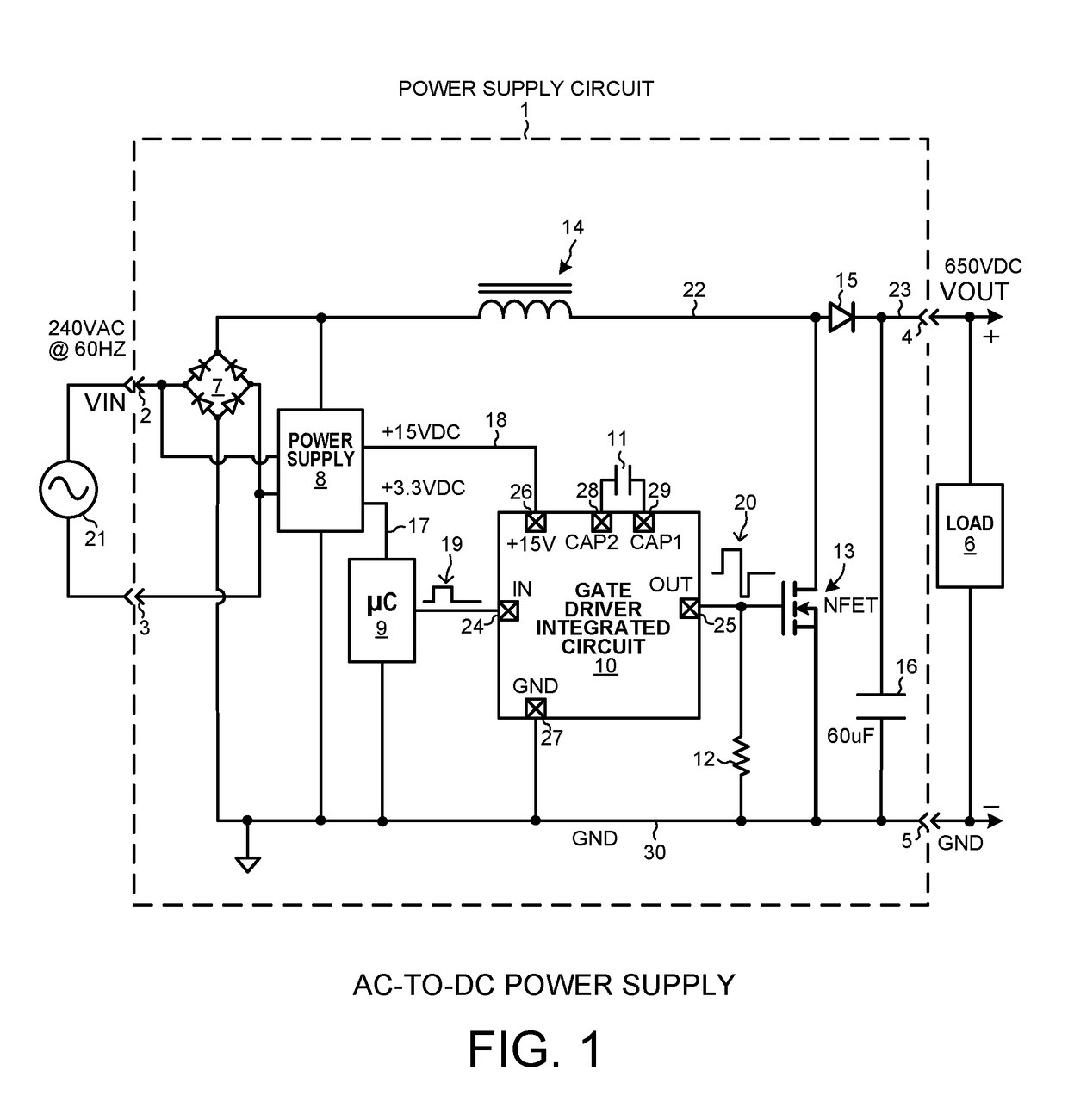
[0055]FIG. 9 is a circuit diagram of a gate driver integrated circuit. This embodiment has a negative supply voltage terminal (labeled −Vcc in the diagram) and employs passive charging to ground potential. This is a terminal of the gate driver integrated circuit. There is no active grounding circuit, but rather in the third period of time the output terminal OUT (and on the gate of the NFET being driven) is charged from the negative supply voltage up to ground potential via resistor R. The voltage on the gate of the NFET is raised up to ground potential at the beginning of the third period of time with an RC circuit waveform as determined by the resistance of the resistor R and the capacitance of the gate of the NFET. The resistor R can be provided on-chip as illustrated, or can be provided external to the gate driver integrated circuit.

[0056]FIG. 10 is a circuit diagram of a third embodiment of a gate driver integrated circuit. This embodiment also has a negative supply voltage ter...

fourth embodiment

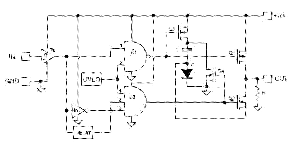
[0057]FIG. 11 is a circuit diagram of a gate driver integrated circuit. This embodiment does not have and does not need a negative supply voltage terminal −VCC. Rather, a capacitor C is used in a charge pump fashion to generate the necessary negative voltage on-chip. The capacitor C can be provided on-chip, or can be provided off chip by providing two capacitor connection terminals CAP1 and CAP2 as shown in FIG. 2. The embodiment of FIG. 11 does not have an active grounding circuit. Rather, the grounding of the gate of the NFET to ground potential during the third period of time is performed by the resistor R. The resistor R can be provided on-chip as illustrated, or can be provided external to the gate driver integrated circuit.

[0058]FIG. 12 is a circuit diagram of a level shifter circuit suitable for use as the level shifter circuit in the embodiment of FIG. 9 and in the embodiment of FIG. 10. The +15V terminal is not really a terminal, but rather denotes a connection to a conduct...


PUM


Abstract

A gate driver integrated circuit drives an output signal onto its output terminal and onto the gate of a power transistor. In a turn-on episode, a digital input signal transitions to a digital logic high level. In response, the gate driver integrated circuit couples the output terminal to a positive supply voltage terminal, thereby driving a positive voltage onto the gate of the power transistor. In response to a high-to-low transition of the digital input signal, the driver drives a negative voltage onto the output terminal and power transistor gate for a short self-timed period of time, and then couples the output terminal to a ground terminal, thereby driving the output terminal and power transistor gate up to ground potential. The output terminal and power transistor gate are then held at ground potential in anticipation of the next turn-on episode of the power transistor.

Description

TECHNICAL FIELD[0001]The described embodiments relate to gate drivers for driving the gates of transistors such as power field effect transistors (so-called MOSFETs) and power Insulated Gate Bipolar Transistors (IGBTs).BACKGROUND INFORMATION[0002]In the design of switching power supplies, such as AC-to-DC switching power supplies in the 5 kW to 10 kW range usable in driving the motors of commercial air conditioners, there has always been a general desire to reduce the cost of the power supply. Despite this, power supply designs continue to have certain characteristics and standard design aspects. Cost often remains undesirably high, despite the desire to reduce it, because how to reduce the power supply manufacturing cost has been, and continues to be, an unknown and nonobvious thing. There are many different parts and aspects of a power supply to be focused on and to which effort can be devoted in the quest to reduce cost. Changing the design of one part of the circuit may actually...

Claims


Application Information

Patent Timeline
IPC IPC(8): H03K3/012H03K19/0185
CPCH03K19/018507H03K3/012H03K17/687H03K2217/0063
Inventor TSYRGANOVICH, ANATOLIY V.NEYMAN, LEONID A.
Owner LITTELFUSE INC
Learn More