

Multilayer printed wiring board production method, adhesive layer-equipped metal foil, metal-clad laminate, and multilayer printed wiring board
a multi-layer printed, wiring board technology, applied in the direction of photosensitive material processing, photomechanical equipment, instruments, etc., can solve the problem of difficult bore, achieve good adhesiveness, enhance the production efficiency of multi-layer printed wiring board having a fine outer layer circui
- Summary
- Abstract
- Description
- Claims
- Application Information
AI Technical Summary
Benefits of technology
Problems solved by technology
Method used
Image

Examples
production example 1
[0121]Respective components as described below were mixed to obtain a varnish of a resin composition A for adhesive layer (solid concentration: about 70% by mass).
[Thermosetting Resin]
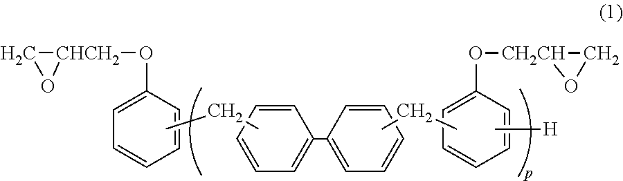
[0122]Novolak type epoxy resin having a biphenyl structure: NC-3000-H (trade name, manufactured by Nippon Kayaku Co., Ltd.): 100 parts by mass
[Polymer Component]
[0123]Carboxylic acid-modified acrylonitrile butadiene rubber particle: XER-91SE-15 (trade name, manufactured by JSR Corporation): 10 parts by mass
[Epoxy Resin Curing Agent]
[0124]Triazine ring-containing cresol novolak type phenol resin: PHENOLITE (registered trademark) LA-3018-50 (trade name, nitrogen content: 18% by mass, hydroxyl group equivalent: 151 g / mol, manufactured by DIC Corporation): 70 parts by mass
[Curing Accelerator]
[0125]Imidazole derivative compound (1-cyanoethyl-2-phenyl imidazolium trimellitate): 2PZ-CNS (trade name, manufactured by Shikoku Chemicals Corporation): 1 part by mass
[Solvent]
[0126]Methyl ethyl ketone
[Production of ...
example 1
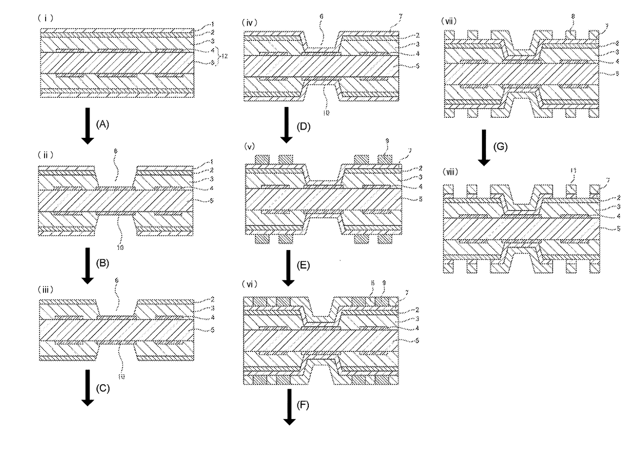
[0127]On the surface of an ultrathin copper foil having a copper foil as a support (copper foil thickness of support: 18 μm, thickness of ultrathin copper foil: 3 μm, manufactured by Mitsui Mining & Smelting Co., Ltd., trade name: MT18Ex-3, surface roughness of roughened surface Rz=2.0 μm), the varnish of the composition A for adhesive layer obtained in Production Method 1 was applied and dried at 170° C. for about 10 minutes, thereby obtaining an ultrathin copper foil with adhesive layer. A thickness of the formed organic adhesive layer was 3.0 μm.
[0128]Subsequently, on both surfaces of a substrate with inner layer circuit, on both surfaces of which a blackening-treated inner layer circuit had been formed (material quality: copper, thickness of circuit: 18 μm (on the both surfaces)) (manufactured by Hitachi Chemical Co., Ltd., trade name: MCL-679FG, thickness: 0.5 mm), the above-obtained ultrathin copper foil with adhesive layer was superimposed such that the organic adhesive layer...
production example 2
[0144]Respective components as described below were mixed using a dispersing machine (manufactured by Yoshida Kikai Co., Ltd., trade name: NANOMIZER (registered trademark)) to obtain a varnish of a resin composition B for adhesive layer (solid concentration: about 35% by mass).
[Thermosetting Resin]
[0145]Novolak type epoxy resin having a biphenyl structure: NC-3000S-H (trade name, manufactured by Nippon Kayaku Co., Ltd.): 100 parts by mass
[Polymer Component]
[0146]Carboxylic acid-modified acrylonitrile butadiene rubber particle: XER-91SE-15 (trade name, manufactured by JSR Corporation): 10 parts by mass
[Epoxy Resin Curing Agent]
[0147]Triazine ring-containing cresol novolak type phenol resin: PHENOLITE (registered trademark) LA-3018-50 (trade name, nitrogen content: 18% by mass, hydroxyl group equivalent: 151 g / mol, manufactured by DIC Corporation): 70 parts by mass
[Curing Accelerator]
[0148]1,8-Diazabicycloundecene (DBU) (manufactured by Kanto Chemical Co., Inc.): 1 part by mass
[Inorga...
PUM
| Property | Measurement | Unit |
|---|---|---|
| Length | aaaaa | aaaaa |
| Length | aaaaa | aaaaa |
| Length | aaaaa | aaaaa |
Abstract
Description
Claims
Application Information