Mixed cation perovskite

a technology of mixed cation perovskite and perovskite, which is applied in the field of crystalline compounds, can solve the problems of limited use, high energy disorder of mapbi/sub>3/sub>, and unexpectedly low absorption

Active Publication Date: 2018-12-06
OXFORD UNIV INNOVATION LTD
View PDF1 Cites 14 Cited by
  • Summary
  • Abstract
  • Description
  • Claims
  • Application Information

AI Technical Summary

Benefits of technology

[0009]The inventors have discovered a perovskite composition which delivers the ideal absorber material for stable and efficient hybrid tandem solar cells. In particular, the inventors have addressed the issues of forming a photo-stable FA based perovskite with the ideal band gap for tandem applications by partially substituting the formamidinium cation with caesium. The remarkable observation has been made that the phase instability region is then entirely eliminated in the iodide to bromide compositional range.

Problems solved by technology

However, to date, there has yet to be a suitable wide band gap top cell material for silicon or thin film technologies, which offers stability, high performance, and low cost.
Although these perovskite structures offer high power conversion efficiencies (PCE), reaching over 20% PCE with band gaps of around 1.5 eV, fundamental issues have been discovered when attempting to tune their band gaps to hit the optimum 1.7 to 1.8 eV range (Yang et al., Science.
The lower band gap regions limit the voltage attainable with such a material, so this band gap “photo-instability” limits the use of MAPb(I(1-y)Bry)3 in tandem devices.
In addition, when considering real-world applications, it has been shown that MAPbI3 is inherently thermally unstable at 85° C., even in an inert atmosphere this is the temperature that international regulations require a commercial PV product to be capable of withstanding.
Furthermore, as the iodide is substituted with bromide, a crystal phase transition is observed from a trigonal to a cubic structure; in compositions close to the transition, the material appears unable to crystallize, resulting in an apparently “amorphous” phase with high levels of energetic disorder and unexpectedly low absorption.
This is not an issue for high efficiency single junction solar cells since they can be fabricated with the iodine rich, phase stable material, but disadvantageously for tandem applications, this occurs right at the Br composition needed to form the desired top-cell band gap of 1.7 to 1.8 eV.
However, their reported efficiencies have yet to surpass the optimized single-junction efficiencies, in part due to non-ideal absorber band gaps having been employed.
However, this method results in a non-ideal efficiency.
However, these perovskite do not yet provide the full tunability and stability required for use in tandem cells.

Method used


Image

  • Mixed cation perovskite
  • Mixed cation perovskite
  • Mixed cation perovskite

Examples


example 2

of Br Content

[0238]Devices containing various perovskites of the formula FA0.83Cs0.17Pb(I(1-x)Brx)3 were synthesis by a method equivalent to that described in Example 1. The PCE of each device was evaluated as for Example 1 and the results are shown in FIG. 33. The devices generally perform well with different bromine contents, and an improvement is observed for contents of over 10%.

example 3

minescence Studies

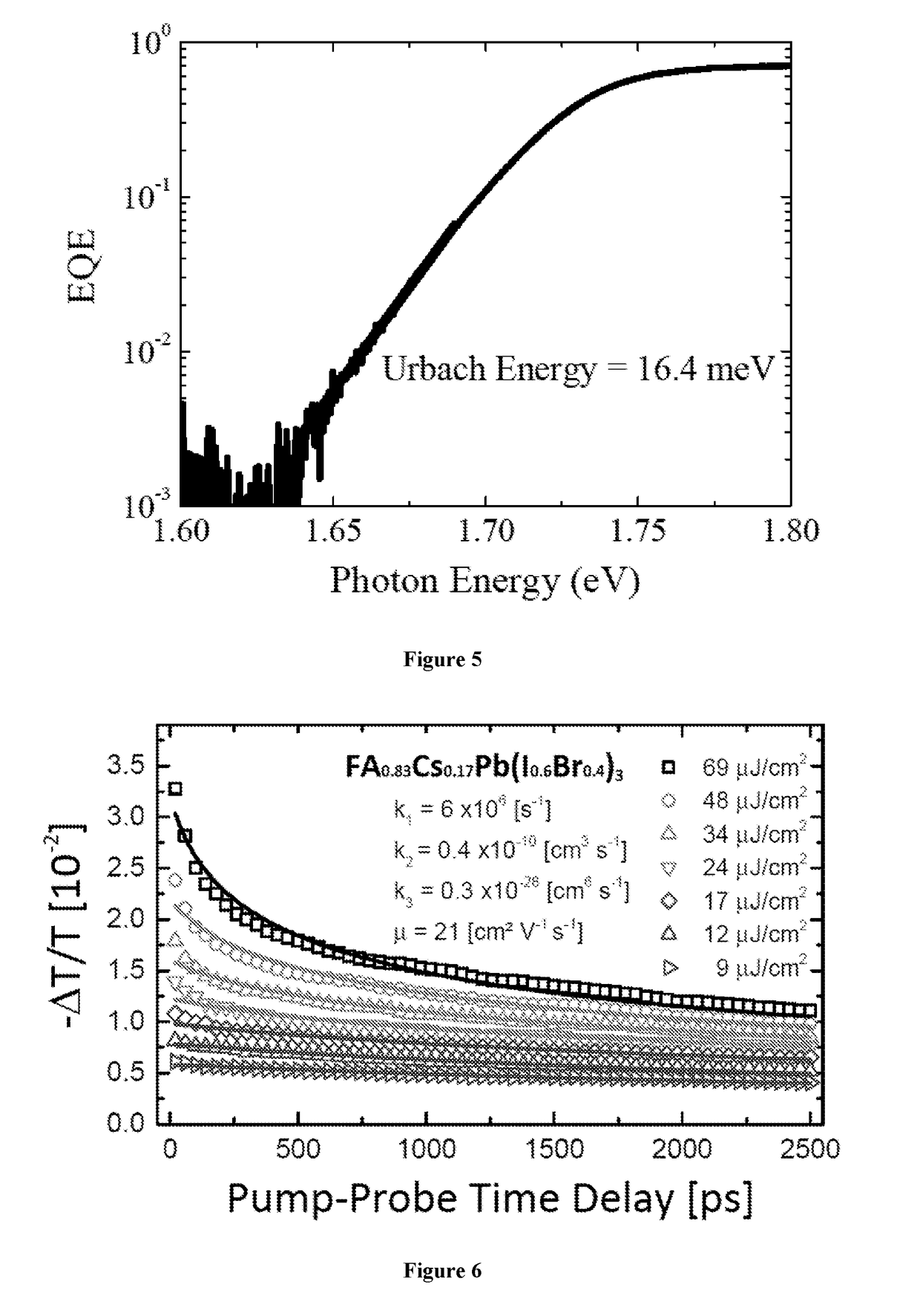
[0239]Examples 1 and 2 concern the photoabsorbent properties of the mixed cation / mixed halide perovskites of the invention. The crystalline compounds of the invention have also been found to be effective photoemissive compounds. As such, light emitting devices could be constructed containing the crystalline compounds of the invention.

[0240]In particular, a series of FA0.825Cs0.175Pb(I(1-x)Brx)3 with x=[0, 0.05, 0.1, 0.2, 0.3, 0.4] devices was prepared following the same fabrication method described for photovoltaic devices. To measure the electroluminescence intensity, the devices were kept in a chamber filled with Nitrogen and placed inside an integrating sphere. The emitted light is collected with a fiber and analysed with a fixed grating CCD spectrometer (Maya Pro, Ocean Optics). The intensity of the luminescence is estimated from the area of the luminescence peak. The current-voltage (IV) properties are measured simultaneously with a Keithley sourcemeter (Model...

example 5

e, Luminescence and XRD Studies of Mixed-Cation Perovskites

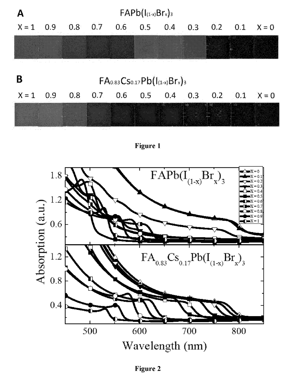
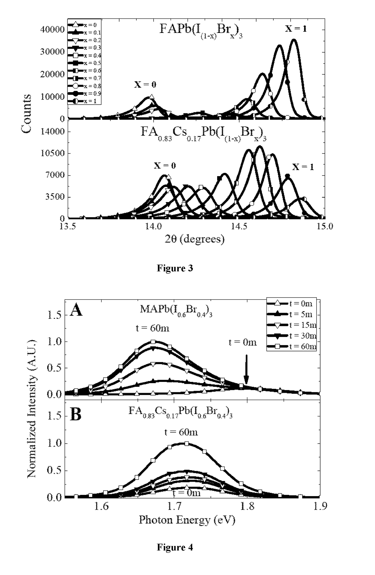
[0245]Layers of FA0.83Cs0.17Pb(ClXBrYIZ)3 perovskites were formed on fluorine-doped tin oxide (FTO) coated glass substrates and annealed at 150° C. for 30 min in nitrogen, using a 0.1M solution dissolved in a 4:1 DMF:DMSO solvent mixture and a nitrogen flow to quench crystallization during spin-coating.

[0246]The UV-vis absorbance spectra of the perovskites were measured and the results are shown in FIG. 38.

[0247]The normalized photoluminescence spectra for the visible range of the perovskites were measured and the results are shown in FIG. 39. Excitation wavelength varied from 375 nm to 600 nm.

[0248]X-ray diffraction patterns (XRD) of the perovskites were measured and the results are shown in FIG. 40.


PUM

PropertyMeasurementUnit
band gapaaaaaaaaaa
thicknessaaaaaaaaaa
band gapaaaaaaaaaa

Abstract

The present invention relates to a crystalline compound comprising: (i) Cs+ (caesium); (ii) (H2N—C(H)═NH2)+ (formamidinium); (iii) one or more metal or metalloid dications [B]; and (iv) two or more different halide anions [X]. The invention also relates to a semiconductor device comprising a semiconducting material, which semiconducting material comprises the crystalline compound. The invention also relates to a process for producing a layer of the crystalline compound.

Description

FIELD OF THE INVENTION[0001]The present invention relates to a crystalline compound useful as a semiconductor material or a photoactive material. The invention also relates to a semiconductor device comprising a semiconducting material, which semiconducting material comprises the crystalline compound. A process for producing a layer of the crystalline compound is also described.[0002]The work leading to this invention has received funding from the EPSRC through the Supergen Solar Energy Hub SuperSolar (EP / M024881 / 1) and (EP / M014797 / 1) the ERC through the Stg-2011 HYPER and the US Office of Naval Research (ONR).BACKGROUND OF THE INVENTION[0003]Terrestrial photovoltaic solar energy, predominantly based on single junction crystalline silicon, has a world record efficiency of 25% which represents an upper limit on the efficiency which we expect commercial modules eventually reach. To go beyond this performance, which is important in order to continuingly drive down the overall cost of g...

Claims


Application Information

Patent Timeline
Patent Type & Authority Applications(United States)
IPC IPC(8): H01L51/44H01L51/00H01L51/42C07F7/24
CPCH01L51/447H01L51/0032H01L51/4226H01L51/0008C07F7/24H10K30/87H10K85/50H10K85/00Y02E10/549H10K30/151H10K71/16
Inventor SALIBA, MICHAELMCMEEKIN, DAVIDSNAITH, HENRY JAMESWENGER, BERNARD
Owner OXFORD UNIV INNOVATION LTD
Why Eureka
Try Eureka