
Nanoprocessing and heterostructuring of silk

Active Publication Date: 2018-12-13
INDIAN INST OF SCI EDUCATION & RES
View PDF0 Cites 1 Cited by
  • Summary
  • Abstract
  • Description
  • Claims
  • Application Information

AI Technical Summary

Benefits of technology

The present invention is a method for seamlessly welding silk fibers with various materials, such as copper, glass, Kevinlar, PVC, PMMA, and PDMS, using a process called "bulging". The method allows for the fabrication of complex microstructures, such as the Mobius strip, chiral helices, and knots. The technique uses optical imaging techniques to confirm the quality of the welds. The technical effect of this invention is the ability to merge silk fibers with other materials in a strong and robust way, paving the way for the fabrication of new functional materials.

Problems solved by technology

So far, there is no known route to merge two silk fibers in air, after they have been spun by the spider.

Method used


Image

  • Nanoprocessing and heterostructuring of silk
  • Nanoprocessing and heterostructuring of silk
  • Nanoprocessing and heterostructuring of silk

Examples


example 1

[0072]Nano-Processing Setup

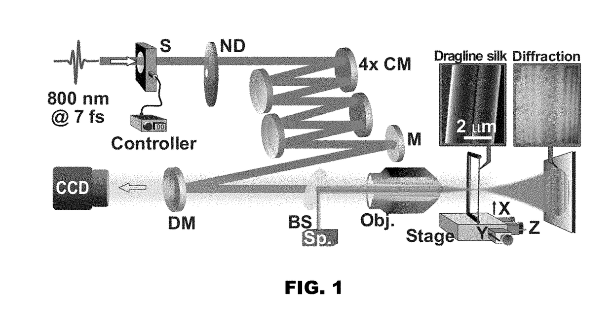
[0073]2 nJ femtosecond-laser system (Femtolaser, Austria) having spectral range of 800 nm, Repetition rate: 85 MHz, and pulse width: 7 fs, S-high speed mechanical shutter (Thorlabs, USA), ND—Neutral density filter (Thor Labs, USA) to control incident intensity, DCM—Dispersion compensated mirrors (Femtolasers, Austria) to maintain the pulse width till focus placed at an angle of 7° to each other. Number of bounces for fs-laser beam was optimized to 4 for maintaining pulse duration of 7-10 fs at focus. DM—Dielectric broadband dichroic mirror (λ=800 nm). Lens—a triplet lens objective having thin glass lens to avoid pulse broadening with Numerical aperture 0.2, The beam spot diameter at focus was about 5 μm. Sample—Stage-Automated X-Y-Z translation stage with a precision of 1 μm, CCD—two high resolution charged couple devices (CCD) were installed, one for diffraction imaging and other in line of focusing for real time monitoring before the dichroic mirror. The...

example 2

[0077]Micro-Welding of Silk with Artificial Materials

[0078]The spider silk was micro-welded to a tissue-like material such as poly-dimethoxysiloxane (PDMS) and contact lens of 9 mm diameter and 600 mg mass Poly (methyl methacrylate) (PMMA) by placing a silk fiber on the edge of fresh (wet) contact lens (FIGS. 6g and 6h). The silk fiber on the lens was exposed to fs pulses such that the damage to contact lens was minimal. This was possible because the contact lens has 500 μm thickness which is much larger compared to the ˜3 μm for silk. The weld joint was sufficiently strong to hold the contact lens in air even when it was dried. This suggests that the silk can be used to “glue” tissue-like materials under ambient conditions without using any chemicals or post processing steps.

[0079]Advantages

[0080]The key advantage of fs pulses is that one can process silk in air with nanoscale precision. Moreover, the key structural building blocks and functionality of silk fibers remain preserved....

example 3

[0081]Micro-Welding of Silk with Artificial Materials

[0082]Methods

[0083]Setup and sample preparation: The 2.2 nJ, 7 fs, 85 MHz pulses at 800 nm central wavelength were produced from the Rainbow oscillator (Femtolasers). Two pairs of chirp mirrors compensated the positive dispersion of the triplet lens objective (NA=0.2, working distance 1.7 mm) and delivered the sub-10 fs short pulses at the focus. The 1 / e2 focal diameter was about 5 μm.

[0084]The dragline silks, diameter 1-6 nm, were extracted from several lab-grown female spiders (Areneous neoscona). The 2-5 cm long silk samples were mounted on a 3-axis stage (Thorlabs) with both motorized and piezo-control offering a 25 nm minimum step increment. An electromechanical shutter (2 ms rise-time, Thorlabs) controlled the exposure time. The laser power was attenuated by the ND filter (Optical density-4) and measured with a power meter (Thorlabs). The optical diffraction of the silk was recorded on a white screen.

[0085]Optical, Raman and...


PUM

PropertyMeasurementUnit
Lengthaaaaaaaaaa
Timeaaaaaaaaaa
Timeaaaaaaaaaa

Abstract

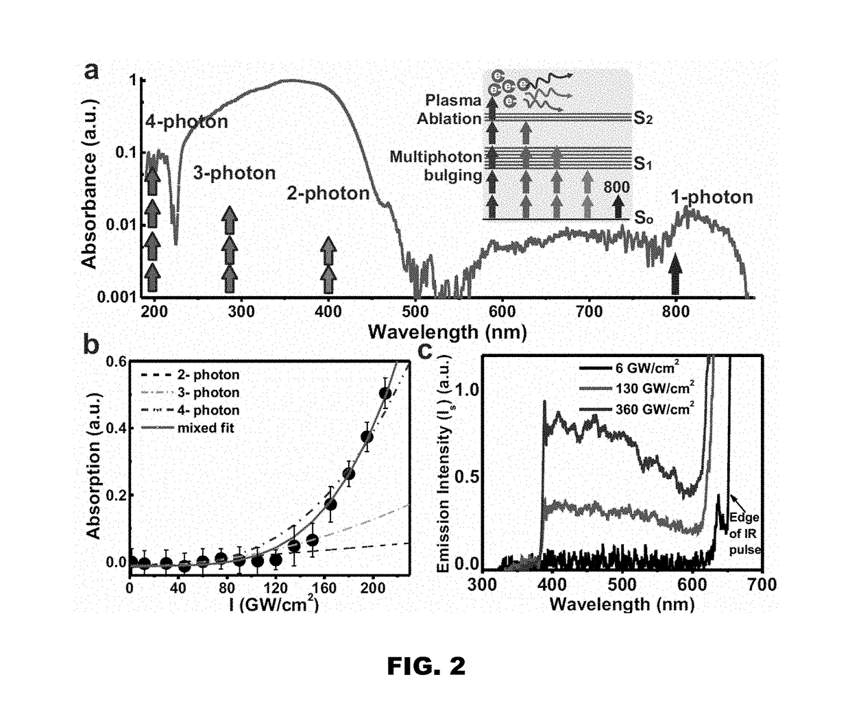
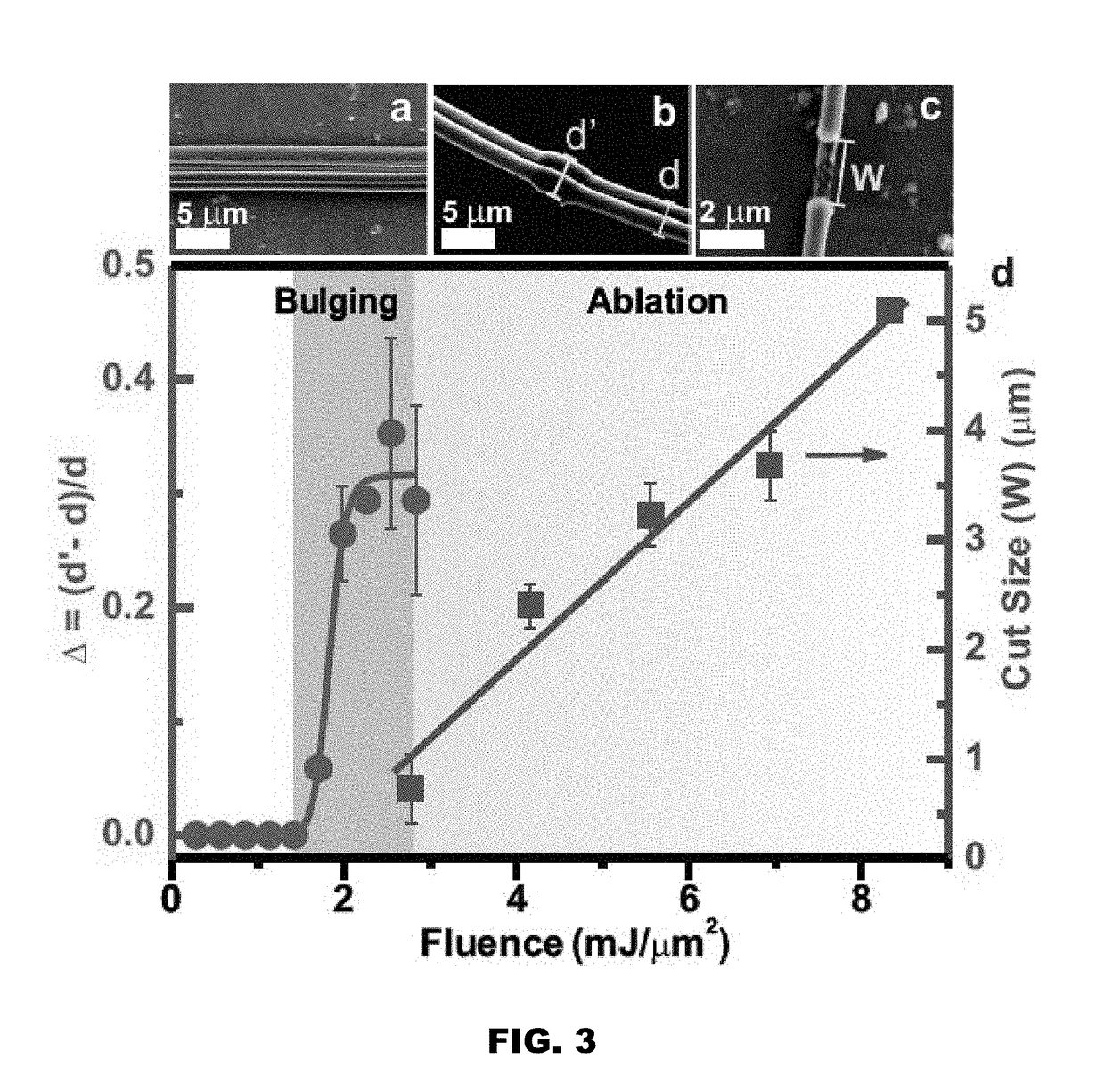
The present invention relates to nanoprocessing and heterostructuring of silk. It has been shown that few-cycle femtosecond pulses are ideal for controlled nanoprocessing and heterostructuring of silk in air. Two qualitatively different responses, ablation and bulging, were observed for high and low laser fluence, respectively. Using this approach, new classes of silk-based functional topological microstructures and heterostructures which can be optically propelled in air as well as on fluids remotely with good control have been fabricated.

Description

CROSS-REFERENCE TO RELATED APPLICATIONS[0001]This application is a continuation-in-part of International Patent Application No. PCT / IB2017 / 051252, filed on Mar. 3, 2017, which published as WO 2017 / 153876 A1 on Sep. 14, 2017, and claims priority of IN201611000500, filed Mar. 6, 2016, the disclosures of each of which are hereby incorporated by reference in their entirety.FIELD OF THE INVENTION[0002]The present invention is in the field of nanotechnology and particularly relates to the nanoprocessing and heterostructuring of natural fibers like silk etc. The present invention involves ultrafast laser based modification and seamless micro-welding of natural fibers including spider silks.BACKGROUND[0003]Spider silk is an ancient biomaterial that is tougher than steel, yet elastic and light weight. The superior physical properties of spider silk make it an attractive biocompatible functional material. Various applications of silk in water collection, biomedical devices and optics have bee...

Claims


Application Information

Patent Timeline
IPC IPC(8): B23K26/00B29C65/00B29C65/16G01Q40/00G01Q70/16B23K26/046B23K26/0622B23K26/06B23K26/03B23K26/22A61L27/22
CPCB23K26/0006B29C66/0224B29C66/0324B29C65/1616B29C66/69B29C66/712B29C66/729G01Q40/00G01Q70/16B23K26/046B23K26/0624B23K26/0626B23K26/032B23K26/22A61L27/227B29K2089/00B29L2031/40B29K2083/00B29L2011/0041B29K2033/12B81C1/00126B81C2201/038
Inventor SINGH, KAMAL PRIYASIDHU, MEHRA SINGHKUMAR, BHUPESH
Owner INDIAN INST OF SCI EDUCATION & RES
Learn More