Semiconductor device and electric apparatus using same

Active Publication Date: 2019-01-03
IDEMITSU KOSAN CO LTD
View PDF0 Cites 1 Cited by
  • Summary
  • Abstract
  • Description
  • Claims
  • Application Information

AI Technical Summary

Benefits of technology

The semiconductor device described in this patent has a designed carrier concentration and a designed withstand voltage that are lower than conventional devices, which results in improved performance and stability. The device also has a unique structure that reduces leak current and allows for easier use of the Schottky electrode in the lower part of the semiconductor layer. Additionally, the device has a lower resistance and can be used in a uni-polar type power device. The withstand voltage per L of the device is preferably 0.5 MV / cm or more, which ensures a higher level of safety and reliability.

Problems solved by technology

On the other hand, they are basically used in the form of monocrystals, and therefore they have drawbacks that growth of the monocrystals on different substrates is difficult and selection of the substrates is limited.
However, inconformity of lattices is large, and hence it is difficult to achieve epitaxial growth of the monocrystals with less defects on Si at a high yield ratio.
The inconformity of lattices of GaN to Si is not as bad as that of SiC, but the crystal growth is difficult unless a buffer layer such as AlN is interposed therebetween, which disturbs the mass production.
However, in an amorphous or polycrystal semiconductor, it is difficult to control the carrier concentration:

Method used


Image

  • Semiconductor device and electric apparatus using same
  • Semiconductor device and electric apparatus using same

Examples


example 1

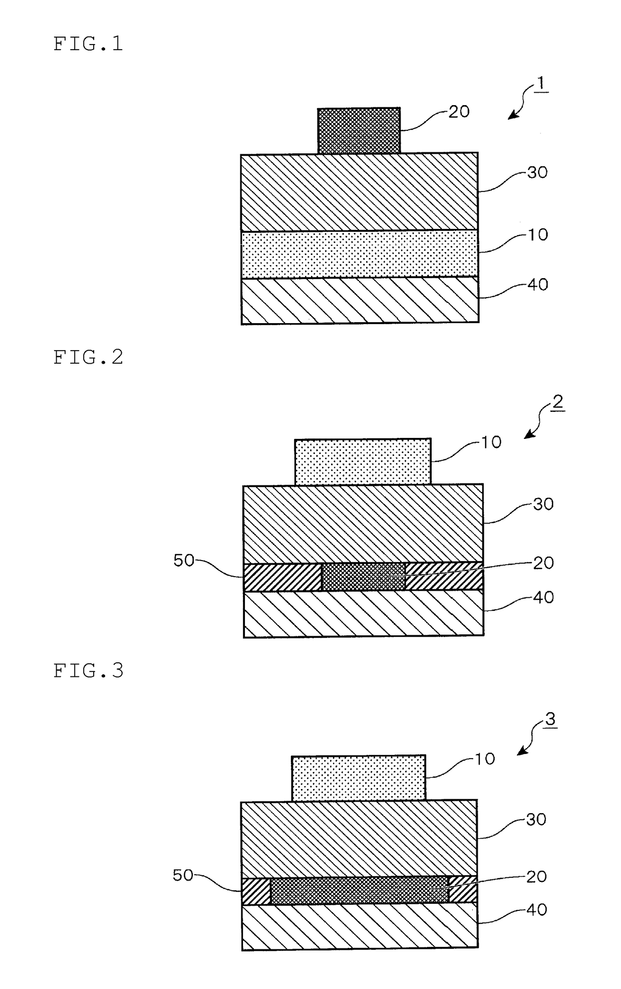
[0145]An n-type Si substrate having a resistivity of 0.001 Ω·cm (a diameter of 4 inches and a thickness of 250 μm) was disposed in a sputtering apparatus (E-2005 manufactured by Anelva Corporation), and the following laminated electrode was formed. Additionally, a substrate back surface was treated with 100 nm of Ti / 50 nm of Au to eliminate a contact resistance with a prober at measurement. Initially, a film of Ti was formed in a thickness of 15 nm with DC of 50 W in an Ar atmosphere, next a film of Pd was formed in a thickness of 50 nm with DC of 50 W in the Ar atmosphere, and finally, as a Schottky electrode, a film of PdO was formed in a thickness of 20 nm with DC of 50 W in a mixed gas atmosphere of Ar and O2.

[0146]Next, this substrate was set together with an areamask for a semiconductor in a sputtering apparatus (CS-200 manufactured by ULVAC), and as a withstand voltage layer (a semiconductor layer), a film of InGaZnO was formed in a thickness of 200 nm (In:Ga:Zn (atom ratio)=...

examples 2 to 5 , 9 , 18 and 19

Examples 2 to 5, 9, 18 and 19

[0174]The procedure of Example 1 was repeated except that film forming conditions were changed as shown in Tables 2-1 and 2-2, to manufacture and evaluate semiconductor devices. Tables 2-1 and 2-2 show the results. Furthermore, the semiconductor devices of these examples satisfied the formula (I).

example 6

[0175]The procedure of Example 1 was repeated except that film forming conditions were changed as shown in Table 2-1, to manufacture and evaluate a semiconductor device. Table 2-1 shows the result. Additionally, the semiconductor device of this example satisfied the formula (I).

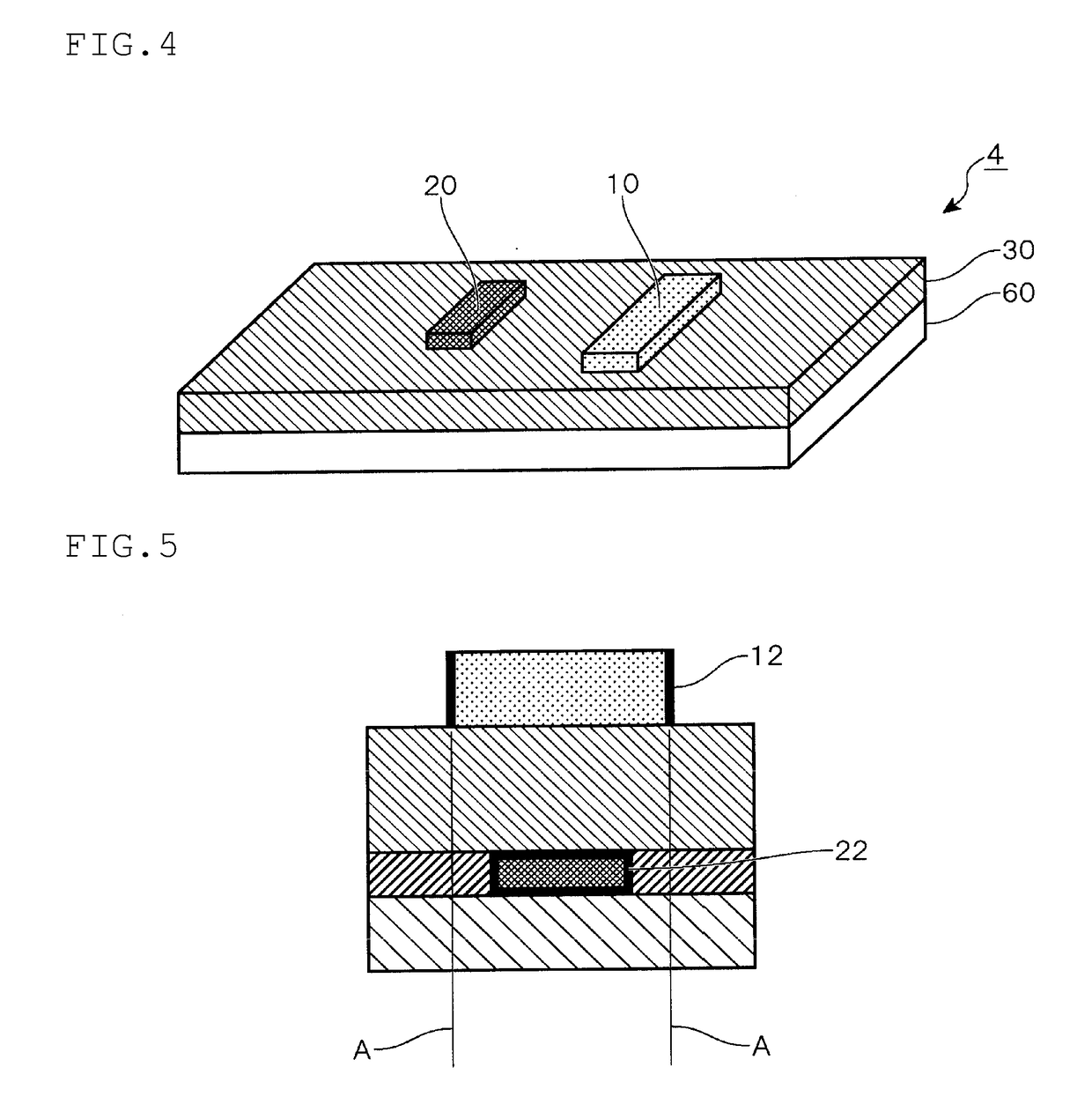
[0176]In this example, a material of the ohmic electrode of Example 1 was changed from Mo to Ti.

[0177]When the L was evaluated, contrast of a TEM image containing InGaZnO was shorter than 200 nm due to extraction of oxygen from the Ti electrode, and it was confirmed that a thickness of a semiconductor layer was 180 nm.


PUM


Abstract

A semiconductor device 1 which comprises a pair of an ohmic electrode 20 and a Schottky electrode 10 separated from each other, and a semiconductor layer 30 in contact with the ohmic electrode 20 and the Schottky electrode 10, and which satisfies the following formula (I):n<ɛVeqL2(I)in which n is a carrier concentration (cm−3) of the semiconductor layer, ε is a dielectric constant (F / cm) of the semiconductor layer, Ve is a forward effective voltage (V) between the ohmic electrode and the Schottky electrode, q is an elementary charge (C), and L is a distance (cm) between the ohmic electrode and the Schottky electrode.

Description

TECHNICAL FIELD[0001]The invention relates to a semiconductor device, and a Schottky barrier diode, a junction transistor, an electronic circuit as well as an electric apparatus using the semiconductor device.BACKGROUND ART[0002]As power semiconductor materials to actualize large current and low power consumption, Si can first be enumerated, and new materials of SiC, GaN and others can also be enumerated. In addition, gallium oxide and diamond are also promising as next generation materials. On the other hand, they are basically used in the form of monocrystals, and therefore they have drawbacks that growth of the monocrystals on different substrates is difficult and selection of the substrates is limited.[0003]With respect to SiC, a preferable crystal structure as the power semiconductor is 4H—SiC, and as dielectric breakdown field of the same, 3 MV / cm or more is actualized. However, inconformity of lattices is large, and hence it is difficult to achieve epitaxial growth of the mon...

Claims


Application Information

Patent Timeline
IPC IPC(8): H01L29/24H01L29/47H01L29/872H01L21/02H01L29/812
CPCH01L29/247H01L29/47H01L29/872H01L21/02565H01L29/812H01L29/45H01L21/02381H01L21/02631H01L29/24H01L29/517
Inventor TSURUMA, YUKISEKIYA, TAKASHITOMAI, SHIGEKAZUKAWASHIMA, EMIUEOKA, YOSHIHIRO
Owner IDEMITSU KOSAN CO LTD
Why Eureka
Try Eureka