
Thin-film transistor and fabrication method thereof and array substrate
a technology of thin-film transistors and fabrication methods, applied in the field of display technology, can solve the problems of the size of a thin-film transistor, and achieve the effects of improving the electrical performance improving the bending durability of the thin-film transistor, and reducing the area of a pixel
- Summary
- Abstract
- Description
- Claims
- Application Information
AI Technical Summary
Benefits of technology
Problems solved by technology
Method used
Image

Examples
Embodiment Construction
[0055]To further expound the technical solution adopted in the present invention and the advantages thereof, a detailed description will be given with reference to the preferred embodiments of the present invention and the drawings thereof.
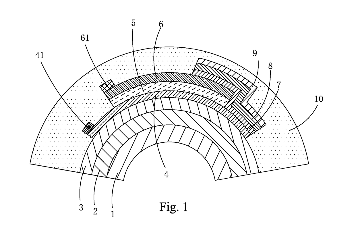
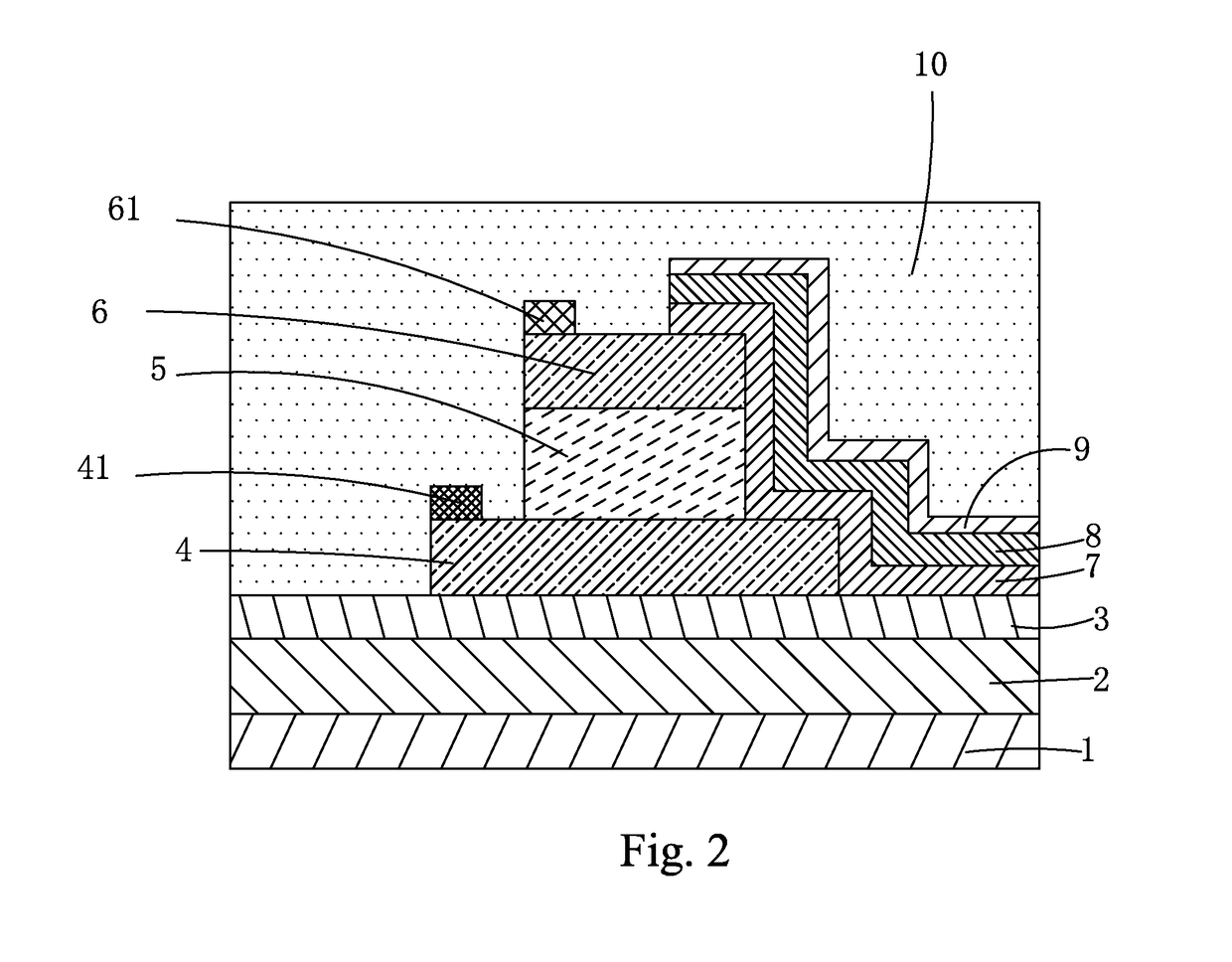
[0056]Referring to both FIGS. 1 and 2, firstly, the present invention provides a thin-film transistor, which comprises:
[0057]a flexible backing 1;
[0058]a moisture / oxygen barrier layer 2 arranged on the flexible backing 1;
[0059]a buffer layer 3 arranged on the moisture / oxygen barrier layer 2;
[0060]a source electrode 4 arranged on the buffer layer 3;
[0061]a separation layer 5 arranged on the source electrode 4 and exposing at least one side portion of the source electrode 4;
[0062]a drain electrode 6 arranged on the separation layer 5;
[0063]an oxide semiconductor channel layer 7 arranged at one side of the separation layer 5 and the drain electrode 6 to sequentially contact a portion of an upper surface of the drain electrode 6, a side surface of the...
PUM
 Abstract
Description
Claims
Application Information