Inductively Coupled Plasma For Hydrogenation of Type II Superlattices

a superlattice and inductive coupling technology, applied in the direction of climate sustainability, sustainable manufacturing/processing, electric discharge tubes, etc., can solve the problems of spatial noise, decrease the detectivity of photodiodes, and increase noise, and achieve easy scaling, high production throughput, and large area fpas

Active Publication Date: 2019-05-02
SIVANANTHAN LAB INC
View PDF6 Cites 0 Cited by
  • Summary
  • Abstract
  • Description
  • Claims
  • Application Information

AI Technical Summary

Benefits of technology

[0012]The exemplary embodiments of the process and apparatus of the invention uses inductively coupled hydrogen plasmas to generate and incorporate hydrogen into semiconductor workpieces, such as type II superlattices. The exemplary embodiments of the process and apparatus of the invention will generate desirable improvements of type II superlattice material and devices, such as increased carrier mobility, increased carrier lifetime, and reduced dark current.
[0016]The exemplary passivation method has the potential to not only remove the deleterious effects of bulk material defects, but also improve surface passivation. This is important because as the detector (pixel) size is reduced, the device's surface area to volume ratio increases and surface leakage current mechanisms become more significant and hence need to be carefully considered and addressed. This is especially true for the long-wavelength infrared (LWIR) and very long-wavelength infrared (VLWIR) detectors, with cutoffs extending beyond 14 □m.
[0018]The exemplary method of generating and incorporating hydrogen into T2SL is suitable for large area FPAs and easily scalable to simultaneously treat multiple FPAs if needed to accommodate high production throughput.
[0019]The exemplary method of the invention provides a process to generate and introduce hydrogen from the inductively coupled plasma system, into a type II superlattice wafer. The type II superlattice wafer can contain a number of detectors formed on one of its faces. These detectors may be fully fabricated or at various stages in their forming process. The process can use hydrogen plasma with a total chamber pressure of 20-300 mTorr, a hydrogen gas flow of 50-100 sccm, an ICP power of 100-900 W, a secondary RF power of 15-90 W, and a process duration adjusted to maximize the benefit of hydrogenation (typically between several tens and several hundreds of seconds). The process can introduce a secondary gas, besides hydrogen, whether simultaneously, or in alternating time intervals, to facilitate the plasma ignition, hydrogen ionization and recombination processes or hydrogen diffusion and impingement onto the processed wafer. The electrostatic chuck can be temperature controlled. The process can provide that He gas is flowed onto the backside of the wafer placed onto the electrostatic chuck to create a gas cushion that improves the thermal contact between the temperature-controlled chuck and the processed wafer.

Problems solved by technology

Defects intersecting the electrical junction may contribute to shunt, tunneling and generation-recombination dark current components, increasing the noise, and subsequently decreasing the detectivity of photodiodes.
Defects and their random distribution generate spatial noise and limit photogenerated current collection in focal plane arrays (FPAs).
Even so, the thermal stability has generally not been found to be so great as to make hydrogen passivation a major tool in the fabrication of high performance semiconductor-based devices.
The exact mechanisms by which hydrogen passivates deep levels are poorly understood, in part due to the lack of a clear understanding of the microscopic nature of many deep levels.
Photodiodes exposed to UV illumination from a high-pressure mercury lamp exhibited degradation in their performance caused by the light or radiation absorbed in the ZnS layer.

Method used


Image

  • Inductively Coupled Plasma For Hydrogenation of Type II Superlattices

Examples


Embodiment Construction

[0022]While this invention is susceptible of embodiment in many different forms, there are shown in the drawings, and will be described herein in detail, specific embodiments thereof with the understanding that the present disclosure is to be considered as an exemplification of the principles of the invention and is not intended to limit the invention to the specific embodiments illustrated.

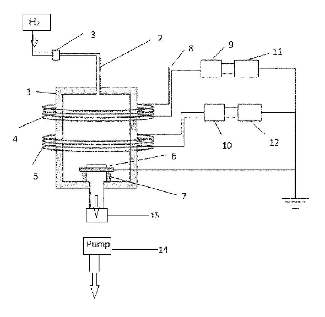
[0023]The hydrogen passivation of defects in T2SL wafers, fully fabricated photodiodes and FPAs is performed using an ICP system operating at 13.56 MHz. An ICP process using only hydrogen gas (H2) has proven effective in generating the hydrogen passivant, maintaining the T2SL surface morphology and avoiding cross-contamination. ICP ensures a high plasma density, conferring a high density of atomic hydrogen at low operating pressures. The hydrogen species generated within the plasmas act as passivants. The plasma exposure typically takes place while the sample resides on a grounded electrode.

[0024...


PUM


Abstract

A process and apparatus is provided to generate and introduce hydrogen from an inductively coupled plasma system into a type II superlattice wafer. The type II superlattice wafer can contain a number of detectors formed on one of its faces. The process can use hydrogen plasma with a total chamber pressure of 20-300 mTorr, a hydrogen gas flow of 50-100 sccm, an ICP power of 100-900 W, a secondary RF power of 15-90 W, and a process duration adjusted to maximize the benefit of hydrogenation (typically between several tens and several hundreds of seconds). The process can introduce a secondary gas to facilitate the plasma ignition, hydrogen ionization and recombination processes or hydrogen diffusion and impingement onto the type II superlattice wafer.

Description

STATEMENT REGARDING FEDERALLY SPONSORED RESEARCH OR DEVELOPMENT[0001]This invention was made with government support under Order NNX16CP72P awarded by NASA. The government has certain rights in the invention.BACKGROUND OF THE INVENTION[0002]Even when grown under lattice-matched conditions, extended and point native defects of various types, including dislocations, vacancies, antisites and interstitials, can be present in any epitaxially grown semiconductor. Defects intersecting the electrical junction may contribute to shunt, tunneling and generation-recombination dark current components, increasing the noise, and subsequently decreasing the detectivity of photodiodes. Defects in the absorber increase diffusion-limited dark currents with commensurate detectivity drops. Defects and their random distribution generate spatial noise and limit photogenerated current collection in focal plane arrays (FPAs).[0003]Current studies indicate that fast Shockley-Read-Hall (SRH) generation / recomb...

Claims


Application Information

Patent Timeline
Patent Type & Authority Applications(United States)
IPC IPC(8): H01L31/18H01L31/0352H01J37/32
CPCH01L31/1868H01L31/035236H01J37/3211H01J37/32449H01J37/32834H01L31/0304H01L31/03046H01J37/32183H01J37/32715Y02P70/50
Inventor BOIERIU, PAULGREIN, CHRISTOPH H
Owner SIVANANTHAN LAB INC
Why Eureka
Try Eureka