Device For In-Situ Fabrication Process Monitoring And Feedback Control Of An Electron Beam Additive Manufacturing Process

a technology of in-situ fabrication process and feedback control, applied in the field of additive manufacturing, can solve the problems of affecting mechanical properties and the geometry of am-manufactured parts, lack of process repeatability and part quality reproducibility, and non-uniform sublimation or evaporation

Active Publication Date: 2020-07-09
HOWMEDICA OSTEONICS CORP +1
View PDF0 Cites 5 Cited by
  • Summary
  • Abstract
  • Description
  • Claims
  • Application Information

AI Technical Summary

Benefits of technology

[0009]In accordance with an aspect, an in situ monitoring and control device and process are disclosed herein for a High Energy Beam Additive Manufacturing (HEBAM) process, in particular an Electron Beam Additive Manufacturing (EBAM) process. The process, which may be embodied as one or more monitoring and control algorithms and executed via a host machine of the device as disclosed herein, includes automatically detecting or measuring features of interest in the EBAM process using one or more sensors. Such detection or measurement may include analyzing at least one of the liquid melt zone and a processing area via a time-series feedback signal and feedback radiation; electronically imaging at least one of a solidified melted surface and the processing area via the feedback signal and feedback radiation; and analyzing chemical compositions of either one or both of the liquid melt zone and the processing area via feedback radiation. The feedback signal and feedback radiation may be captured by sensors and may be fed into a monitoring controller, which may evaluate the data associated with the detected feedback signal and feedback radiation captured by the sensors to determine any one or any combination of a magnitude, a degree, and a rate of change in monitored features of interest of any one or any combination of the EBAM process, the liquid melt zone, the solidified melted surface, and the processing area. The monitoring controller may then send process control commands to the process controller on the host machine to modify a set of process parameters for the EBAM process. In this manner, execution of the in situ EBAM process monitoring and control algorithms may maintain consistency of the EBAM process.
[0039]In some arrangements, any the electron sensor system may include an electrically conductive sensing surface, electrical-noise filter plates, suitable ceramic components, an instrumentation amplifier, and suitable data loggers. The electrically conductive sensing surface may be configured for the capture of feedback electrons. The electrical-noise filter plates may be configured for noise reduction in the feedback electron signal. The suitable ceramic components may be configured for positioning the one or more electron sensors at a suitable location and may be configured for providing the electrical-noise filter plates with electrical insulation from the electrically conductive sensing surface. The instrumentation amplifier may be configured for providing a suitable signal-to-noise ratio in the feedback electron signal. The suitable data loggers may be configured for sampling and performing suitable signal conditioning to the feedback electron signal and process parameters for the scan apparatus process parameters. The electron sensor system may enclose the processing area to maximize the chance for capturing feedback electrons emitted from the processing area at a wide range of angles.
[0061]In accordance with another aspect, an electron beam and powder bed processing, monitoring, and feedback device for fabricating a build structure in a processing area may include an electron beam generation apparatus, a substrate, a vacuum chamber, an electronic imaging device, a monitoring controller, and an electron beam controller. The electron beam generation apparatus may be configured for generating and deflecting an electron beam over a powder bed within the processing area. The substrate may be configured for supporting a powder bed and the build structure during deflection of the electron beam. The electronic imaging device may be enclosed in the vacuum chamber and may include a first plate electrically insulated from the electron beam generation apparatus. The first plate may include a feedback signal-capturing surface that electrically conducts a first electrical signal upon impingement of impinging electrons emitted from the build structure. The first plate may extend either one or both of over and around the processing area. The monitoring controller may be configured for receiving and interpreting, by one or more processors the first electrical signal, using a first algorithm, to assess the quality of the deposition of the powder bed within the processing area and, using a second algorithm, to assess the quality of a solidified surface of the build structure after sintering or melting a portion of the powder bed within the processing area. The monitoring controller may be further configured for transmitting, by one or more processors, one or more instructional electrical signals corresponding first instructions based on the assessed quality of the deposition of the powder bed when the monitoring controller assesses the quality of the deposition of the powder bed within the processing area and second instructions based on the assessed quality of a solidified surface of the build structure after sintering or melting a portion of the powder bed when the monitoring controller assesses the quality of the solidified surface of the build structure after sintering or melting a portion of the powder bed. The electron beam controller may be configured for receiving and interpreting the one or more instructional electrical signals transmitted by the monitoring controller. The electron beam controller further may be configured for transmitting, based on the received and interpreted instructional electrical signals, electron beam controller electrical signals to modify settings of the electron beam generation apparatus. The modified settings of the electron beam generation apparatus may reduce or eliminate determined differences between any one or any combination of (i) the assessed quality of the deposition of the powder bed and a predefined quality of the deposition of the powder bed and (ii) the assessed quality of a solidified surface of the build structure after sintering or melting a portion of the powder bed and a predefined quality of a solidified surface of the build structure after sintering or melting a portion of the powder bed.
[0065]In some arrangements, the electronic imaging device may be a temperature measurement and electronic imaging device. The temperature measurement and electronic imaging device further may include a thermocouple electrically connected with the first plate. The thermocouple may electrically conduct a thermal energy sensing electrical signal upon receipt of thermal radiation emitted from the build structure. The monitoring controller may be configured for receiving and interpreting, by one or more processors, using an algorithm different from the first and the second algorithms, the thermal energy sensing electrical signal electrically conducted by the thermocouple to assess the temperature of the processing area. The monitoring controller further may be configured for transmitting, by one or more processors, an instructional electrical signal corresponding to thermal energy instructions based on the assessed temperature of the powder bed within the processing area. The modified settings of the electron beam generation apparatus may reduce or eliminate determined differences between the assessed temperature of the powder bed within the processing area and a predefined temperature of the powder bed within the processing area.
[0066]In some arrangements, the electron beam and powder bed processing, monitoring, and feedback device further may include an electromagnetic radiation detection device. The electromagnetic radiation detection device may be mounted in a housing providing vapor protection and thermal regulation. The electromagnetic radiation detection device may be at least partially within the vacuum chamber and may electrically conduct a radiation detection electrical signal upon the detection of electromagnetic radiation emitted from the build structure. The monitoring controller may be configured for receiving and interpreting, by one or more processors, using an algorithm different from the first and the second algorithms, the radiation detection electrical signal electrically conducted by the electromagnetic radiation detection device to assess the chemical composition within the processing area. The monitoring controller further may be configured for transmitting, by one or more processors, an instructional electrical signal corresponding to detected radiation instructions based on the assessed chemical composition within the processing area. The modified settings of the electron beam generation apparatus may reduce or eliminate determined differences between the assessed chemical composition within the processing area and a predefined chemical composition within the processing area.
[0070]In some arrangements, the electron sensor system may include an electrically conductive sensing surface, electrical-noise filter plates, suitable ceramic components, an instrumentation amplifier, and suitable data loggers. The electrically conductive sensing surface may be configured for the capture of feedback electrons. The electrical-noise filter plates may be configured for noise reduction in the feedback electron signal. The suitable ceramic components may be configured for positioning the electron sensor at a suitable location and for providing the electrical-noise filter plates with electrical insulation from the electrically conductive sensing surface. The instrumentation amplifier may be configured for providing a suitable signal-to-noise ratio in the feedback electron signal. The suitable data loggers may be configured to sample and perform suitable signal conditioning to the feedback electron signal and the scan apparatus process parameters. The electron sensor system may enclose the processing area to maximize the chance for capturing feedback electrons emitted from the processing area at a wide range of angles.

Problems solved by technology

Applications of AM techniques in various industries have been met by challenges caused by a lack of process repeatability and part quality reproducibility.
Typical quality issues in AM processes include the formation of undesired porosity on melted surfaces as well as the delamination of layers, both of which affect mechanical properties and the geometry of AM-manufactured parts.
Within an alloy, chemical constituents of the alloy have different thermal properties, meaning that sublimation or evaporation is non-uniform.
This non-uniformity could cause the chemical composition of the powder to be different than that of printed parts.
In the current state of the art, AM machines lack effective in situ process monitoring and control, which hinders the establishment of desired correlations between AM process parameters and AM-manufactured part characteristics, which include part geometry, processing area quality, and the chemical composition of printed parts.
These deficiencies are among the major barriers inhibiting the adoption of AM techniques across industries.
While some in situ process monitoring methods are used for SLAM processes with the PBF set-up, these methods are not suitable for the EBAM process for two main reasons.
First, the physics of interactions between the different energy source, i.e., the laser beam and the electron beam, and the powder itself are sufficiently different such that any in situ monitoring methods associated with a laser heat source are not readily applicable to a process using an electron beam as the heat source.
Secondly, the above-noted sublimation and evaporation of the powder occurs more commonly during the EBAM process which requires a vacuum chamber.
These metallic coatings would reduce the effectiveness or even damage typical SLAM sensors if they were to be integrated into an EBAM apparatus for monitoring and control purposes.
However, this camera system lacks the ability to magnify an individual region of interest on the powder bed without compromising spatial resolution, and further lacks the capability to observe the chemical composition of the printed part or of the powder among other deficiencies.
One of the major inherent drawbacks of collecting and making use of detected radiation with wavelengths either in the visible or IR region is that the spatial resolution near part boundaries of the generated digital optical image is influenced heavily by the radiation emitted from the Heat-Affected Zone (HAZ) surrounding the region of interest.
This emitted radiation might result in blurred part boundaries in the digital optical images and affect the accuracy of part-geometry analysis.

Method used


Image

  • Device For In-Situ Fabrication Process Monitoring And Feedback Control Of An Electron Beam Additive Manufacturing Process
  • Device For In-Situ Fabrication Process Monitoring And Feedback Control Of An Electron Beam Additive Manufacturing Process
  • Device For In-Situ Fabrication Process Monitoring And Feedback Control Of An Electron Beam Additive Manufacturing Process

Examples


application examples

Example 1: Use of Feedback Electron Signal for Observation and Study of the Electron Beam Additive Manufacturing Process

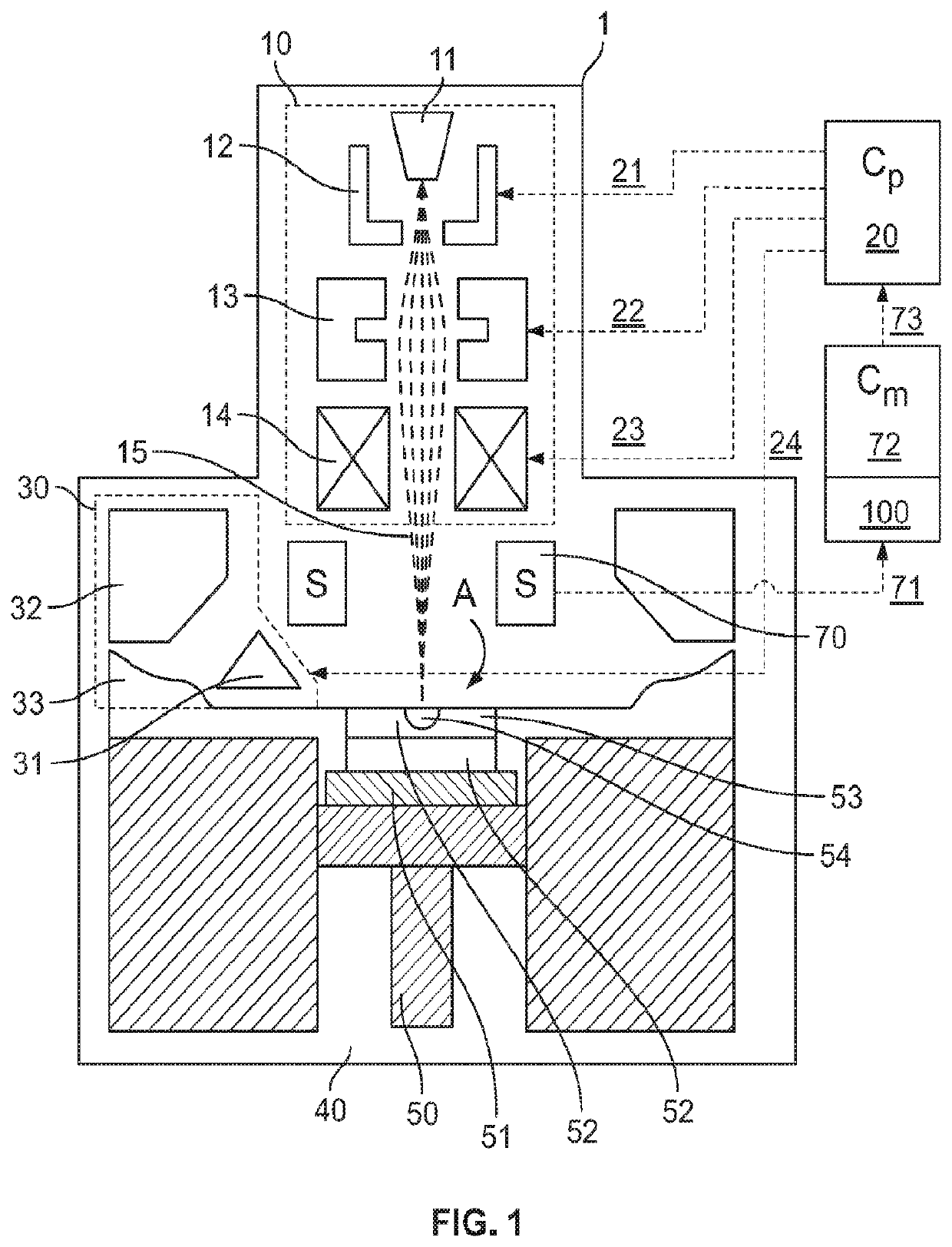
[0100]An in situ monitoring system, such as device 200 configured to operate EBAM process monitoring and feedback control process 400 on host machine 1, may be used to observe and study the interactions between the primary electron beam and processing area, melt zone, powder bed and the solidified melted surface for quality verification. A few experiments were carried out using such a system, in which the primary electron beam was sent to raster-scan across a 200 mm×200 mm×2 mm (Width (W)×Depth (D)×Height (H)) stainless steel plate with a 200 mm×50 mm×2 mm (W×D×H) aluminum plate placed on top. A feedback electron sensor in the monitoring system captured the feedback electrons from the processing area during the beam scan while a data logger sampled the obtained signal and relayed the data to a monitoring controller. FIG. 6 is a plot of typical feedback electron sig...

example 2

edback Thermal Radiation Signal for Observation and Study of the Electron Beam Additive Manufacturing Process

[0101]The in situ monitoring system may be used to observe and study the temperature of the processing area, melt zone, powder bed and the solidified melted surface for quality verification. During an experimental build, an EBAM host machine pre-heated its processing area before fabricating a predefined design in a layer upon layer fashion. A feedback thermal radiation sensor in the monitoring system captured the feedback thermal radiation irradiated from the processing area throughout the build while a data logger sampled the obtained signal and relayed the data to a monitoring controller. FIG. 7 is a plot of feedback thermal radiation signals received from a user-defined region of interest within the EBAM host machine as a function of time. The plot shows that the feedback thermal radiation captured by the sensor gives a pattern which reflects the host machine building step...

example 3

ectronic Imaging for Observation and Study of the Electron Beam Additive Manufacturing Process

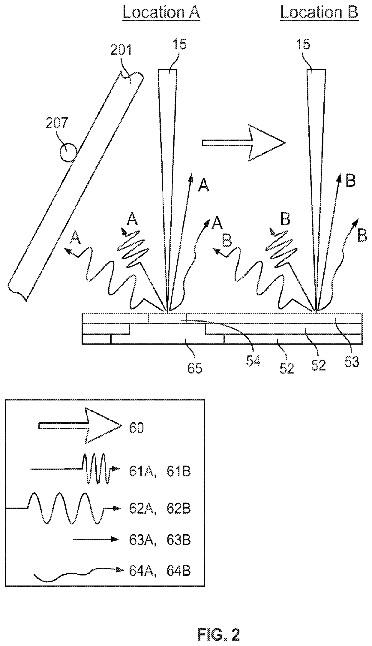
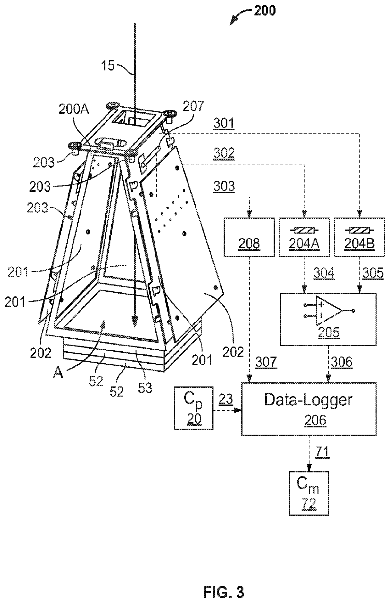
[0102]The in situ monitoring system can be used to observe and study the EBAM process by carrying out electronic imaging. A feedback electron sensor, such as device 200, in the monitoring system captures the feedback electrons from the processing area during electronic imaging while a data logger samples the obtained signal and relays the data to a monitoring controller. The monitoring controller runs algorithms to generate digital electronic images from the data relayed from the data logger. The digital electronic images generated allow quality evaluation of the deposition of powder in the powder bed, anomaly detection in the processing area, and geometry deviation quantification of the solidified melted surface. Various sets of experiments were carried out to verify the electronic imaging capability of the monitoring system.

[0103]One of the experiments concerned monitoring area and spatia...


PUM

PropertyMeasurementUnit
Widthaaaaaaaaaa
sizeaaaaaaaaaa
sizeaaaaaaaaaa

Abstract

A High Energy Beam Processing (HEBP) system provides feedback signal monitoring and feedback control for the improvement of process repeatability and three-dimensional (3D) printed part quality. Signals reflecting process parameters and the quality of the fabricated parts are analyzed by monitoring feedback signals from artifact sources with a process controller which adjusts process parameters. In this manner, fabricated parts are produced more accurately and consistently from powder feedstock by compensating for process variation in response to feedback signals.

Description

CROSS-REFERENCE TO RELATED APPLICATIONS[0001]The present application claims the benefit of the filing date of U.S. Provisional Patent Application No. 62 / 509,464, filed May 22, 2017, the disclosure of which is hereby incorporated herein by reference.FIELD OF THE INVENTION[0002]The present invention generally relates to additive manufacturing, and in particular relates to a system for monitoring, interpreting, and controlling the fabrication of components during High Energy Beam Processing (HEBP).BACKGROUND OF THE INVENTION[0003]Additive Manufacturing (AM) is increasingly used in the development of new products across many industrial sectors such as the medical and aerospace industries. HEBP technologies can be used as one of the AM techniques to build three-dimensional (3D) parts as a series of two-dimensional (2D) layers via a layer-wise computer-controlled production process. HEBP machines used in AM will be referred to as High Energy Beam Additive Manufacturing (HEBAM) machines he...

Claims


Application Information

Patent Timeline
Patent Type & Authority Applications(United States)
IPC IPC(8): B33Y10/00B22F3/105
CPCB33Y40/00B22F3/1055B33Y50/02B22F2999/00B33Y10/00B22F2003/1058B33Y30/00B29C64/153B23K15/0026B23K15/0086B23K15/06G01N23/2252G01N2223/645Y02P10/25B22F10/30B22F12/41B22F10/28B22F10/368B22F12/44B22F10/37B22F12/90H02S40/22Y02E10/52B22F2203/11B22F2202/11H01L31/02164H01L31/02167
Inventor SUTCLIFFE, CHRISTOPHER J.GARRARD, REBECCA HELENJONES, ERICMULLEN, LEWISWONG, HAY
Owner HOWMEDICA OSTEONICS CORP
Why Eureka
Try Eureka