Method for porosifying a material and semiconductor structure
- Summary
- Abstract
- Description
- Claims
- Application Information
AI Technical Summary
Benefits of technology
Problems solved by technology
Method used
Image

Examples
Embodiment Construction
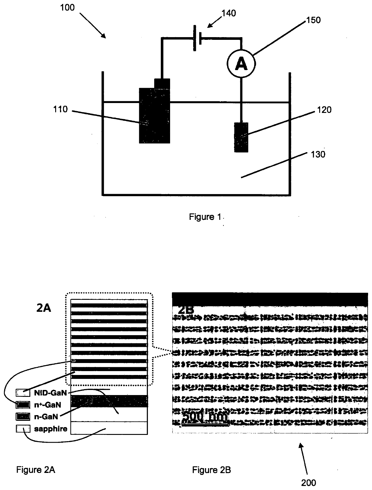
[0162]FIG. 1 shows a schematic of an electrochemical (EC) experimental setup usable in the method of the present invention. As shown in FIG. 1, the experimental setup consists of a two-electrode electrochemical cell 100, with a sample 110 connected as an anode and a platinum foil 120 connected as a cathode. The platinum cathode, and at least a portion of the surface layer of the sample, are exposed to an electrolyte 130 by immersion in the electrolyte. A constant current DC power supply 140 is connected between the anode and the cathode, and an ammeter 150 is used to monitor and record the etching current flowing through the circuit.
[0163]Unless otherwise stated, the EC etching experiments described herein were conducted at room temperature with a semiconductor structure as the anode and a platinum foil as the counter electrode (cathode). Oxalic acid with a concentration of 0.25 M was used as the electrolyte. The etching process was carried out in a constant voltage mode controlled ...
PUM
 Abstract
Description
Claims
Application Information
 - R&D Engineer
- R&D Manager
- IP Professional
- Industry Leading Data Capabilities
- Powerful AI technology
- Patent DNA Extraction
Browse by: Latest US Patents, China's latest patents, Technical Efficacy Thesaurus, Application Domain, Technology Topic.
© 2024 PatSnap. All rights reserved.Legal|Privacy policy|Modern Slavery Act Transparency Statement|Sitemap