

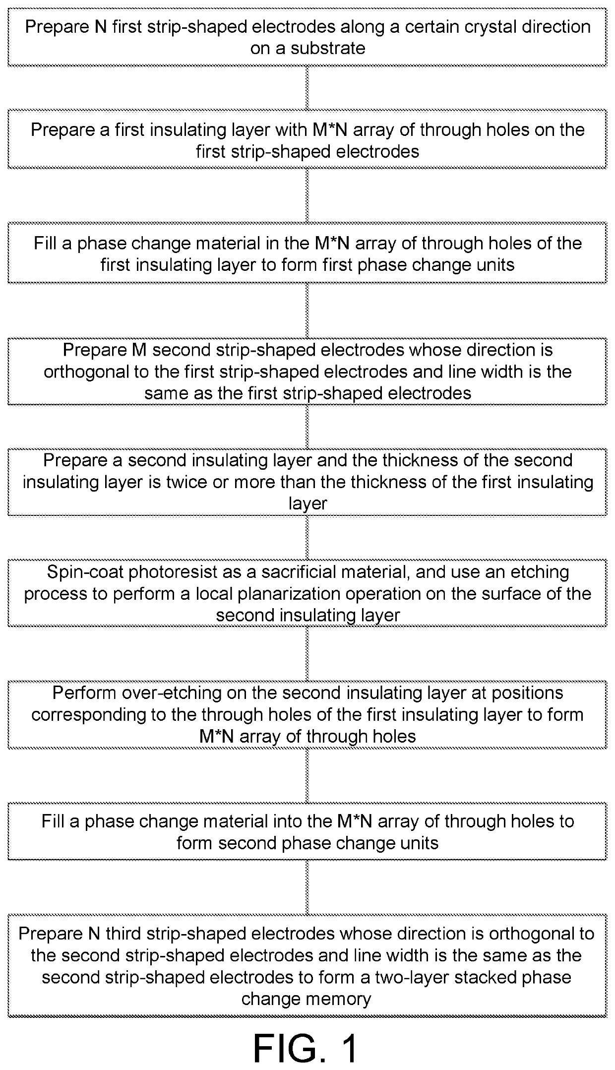
Three-dimensional stacked memory and preparation method thereof
a three-dimensional stacking and memory technology, applied in the field of three-dimensional stacking memory and a preparation method thereof, can solve the problems of material selection, device structure, process implementation difficulty and cost, and two-dimensional planar phase change memory has encountered physical limitations in the reduction of device size, so as to improve heat utilization rate, reduce implementation difficulty, and improve the effect of heat utilization ra
- Summary
- Abstract
- Description
- Claims
- Application Information
AI Technical Summary
Benefits of technology
Problems solved by technology
Method used
Image

Examples
specific embodiment 1
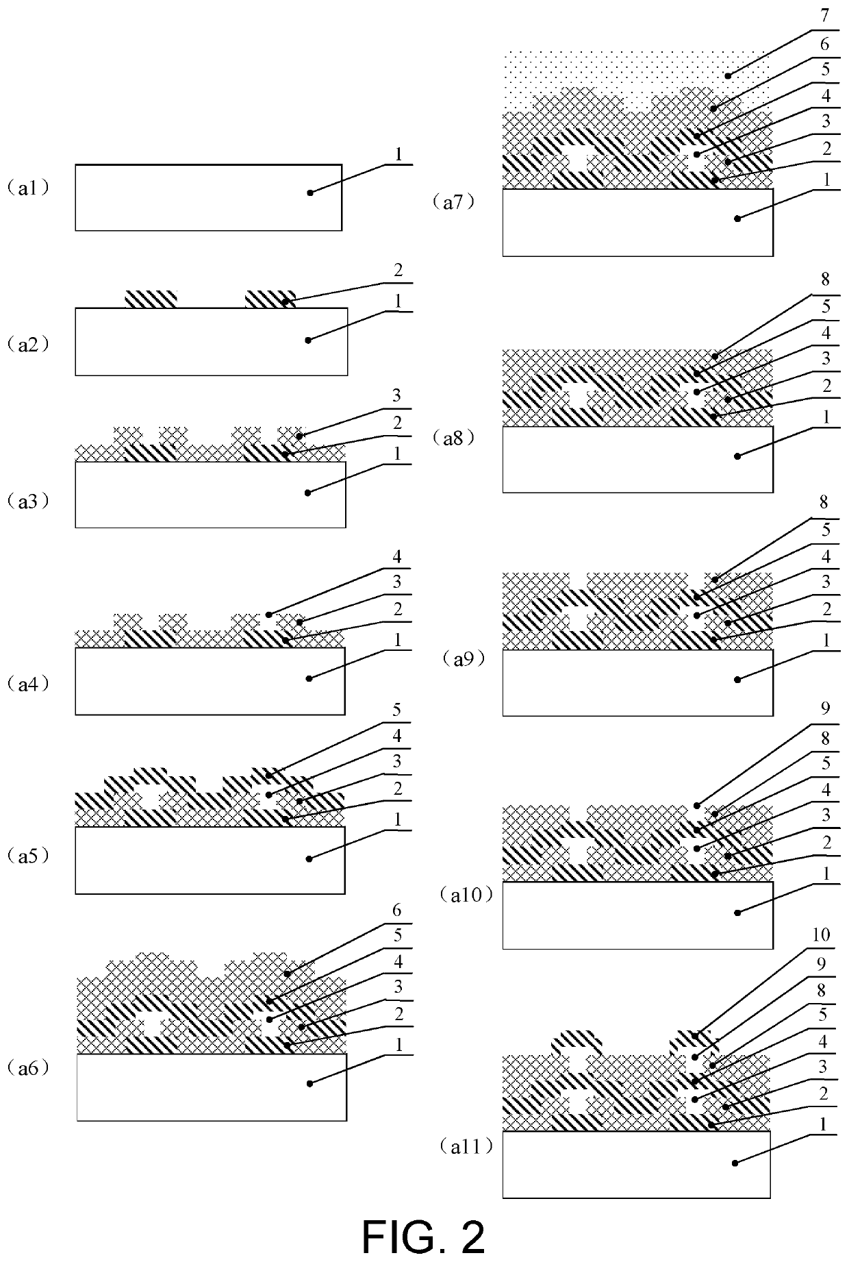
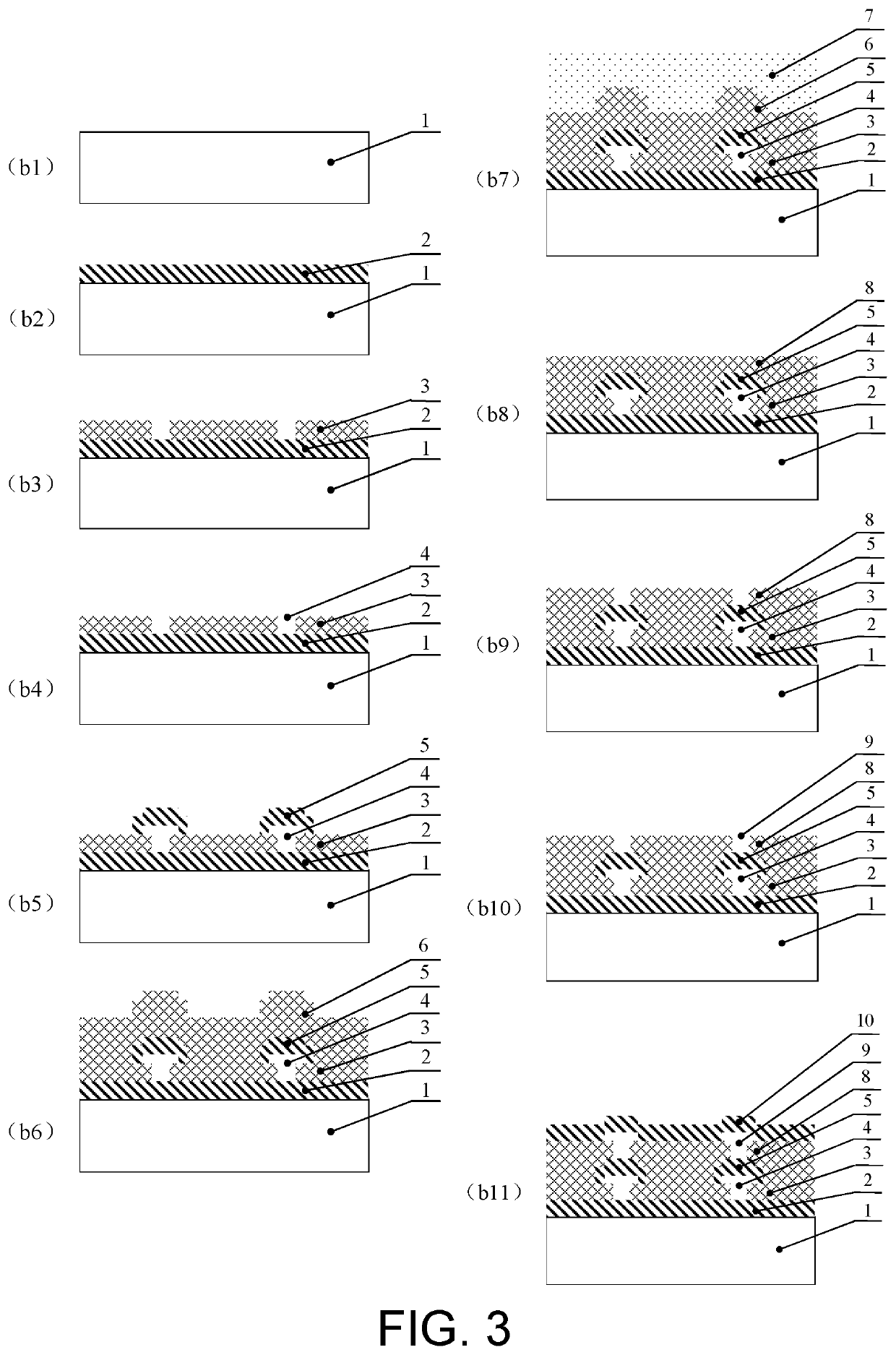
[0070]Step 1: On a silicon substrate 1 with a 1000 nm thick SiO2 oxide layer on its surface, photolithography is performed to obtain a pattern of a number of first strip-shaped electrodes with a line width of 10 μm along a certain crystal direction. A 100 nm thick TiW alloy electrode material is deposited on the substrate after photolithography, and after performing a peeling process, first strip-shaped electrodes 2 corresponding to the photolithographic pattern are obtained, as shown in (a1 to a2) of FIG. 2 and (b1 to b2) of FIG. 3.
[0071]Step 2: On the basis of Step 1, photolithography is performed to obtain a pattern of a rectangular first insulating layer with a larger area and array of through holes. The pattern covers the effective region of the first strip-shaped electrode and exposes the pins at both ends of the first strip-shaped electrode. The size of each of the array of through holes is 4 μm, and all the array of through holes are located on the first strip-shaped electro...
specific embodiment 2
[0080]Step 1: On a silicon substrate 1 with a 1000 nm thick SiO2 oxide layer on its surface, photolithography is performed to obtain a pattern of a number of strip-shaped electrodes with a line width of 6 μm along a certain crystal direction. A 20 nm thick Ti and 80 nm thick Pt electrode materials are deposited in sequence on the substrate after photolithography, and after performing a peeling process, first strip-shaped electrodes 2 corresponding to the photolithographic pattern are obtained, as shown in (a1 to a2) of FIG. 2 and (b1 to b2) of FIG. 3.
[0081]Step 2: On the basis of Step 1, photolithography is performed to obtain a pattern of a rectangular first insulating layer with a larger area and array of through holes. The pattern covers the effective region of the first strip-shaped electrode and exposes the pins at both ends of the first strip-shaped electrode. The size of each of the array of through holes is 2 μm, and all the array of through holes are located on the underlyi...
PUM
 Abstract
Description
Claims
Application Information