On-chip polarization detection and polarimetric imaging

a polarization detection and polarimetric imaging technology, applied in the direction of polarising elements, instruments, optical radiation measurement, etc., can solve the problems of limiting optical performance, miniaturization and device integration, and conventionally difficult to analyze the polarization state of light such as cpl using one single material or device, and achieves low loss and scalability to ultra-compact footprints.

Active Publication Date: 2021-06-24
ARIZONA STATE UNIVERSITY
View PDF0 Cites 13 Cited by
  • Summary
  • Abstract
  • Description
  • Claims
  • Application Information

AI Technical Summary

Benefits of technology

[0019]Among general advantages of embodiments disclosed herein are compatibility with existing silicon-based devices and semiconductor fabrication techniques (including CMOS processes), scalability to ultra-compact footprints, and functionality across wide ranges in wavelength, including mid-infrared, where alternative approaches may perform poorly due to strong material absorption or weak birefringence.
[0020]Some embodiments are capable of circular polarization filtering with extinction ratios of greater than 100 in simulations and have realized circular polarization filtering with extinction ratios higher than 30, transmission efficiencies near 80% for near-infrared wavelengths of 1.3 μm to 1.6 μm with low loss (<0.45 dB) in experimentally fabricated structures.

Problems solved by technology

However, because conventional devices used for light detection (e.g. semiconductor photodetectors) intrinsically lack structural chirality, it is conventionally difficult to analyze the polarization state of light such as CPL using one single material or device.
This poses serious challenges to miniaturization and device integration, and usually further limits the optical performance (introducing loss and constraining bandwidth) of the resulting instrument.
However, organic materials are much less stable in ambient conditions (temperature, humidity, oxygen, light, etc.) compared to inorganic materials, and they considerably constrain the process integration with other materials for more complex functionalities.
Furthermore, the organic materials also have a limited electronic response time and small operational wavelength range.
However, such chiral structures have limited extinction ratio in both absorption and electrical current signals of LCP and RCP (<3.5), and the structural design is rather complicated for large-scale inexpensive fabrication in order to be implemented in practical applications.
Additionally, the hot-electron generation process is usually associated with noise that can degrade the signal-to-noise ratio.
In summary, conventional polarized light detection techniques still require slow and bulky analyzing tools, typically benchtop-sized devices, which operate on the scale of milliseconds.

Method used


Image

  • On-chip polarization detection and polarimetric imaging
  • On-chip polarization detection and polarimetric imaging
  • On-chip polarization detection and polarimetric imaging

Examples


Embodiment Construction

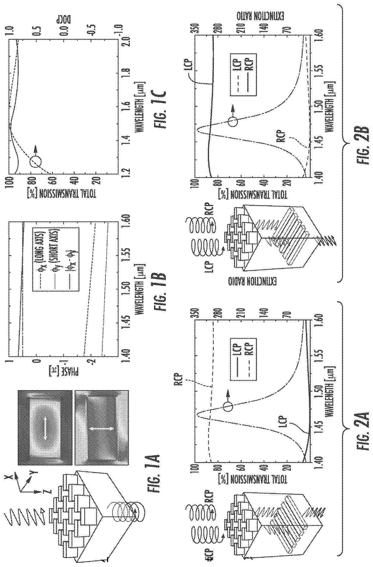
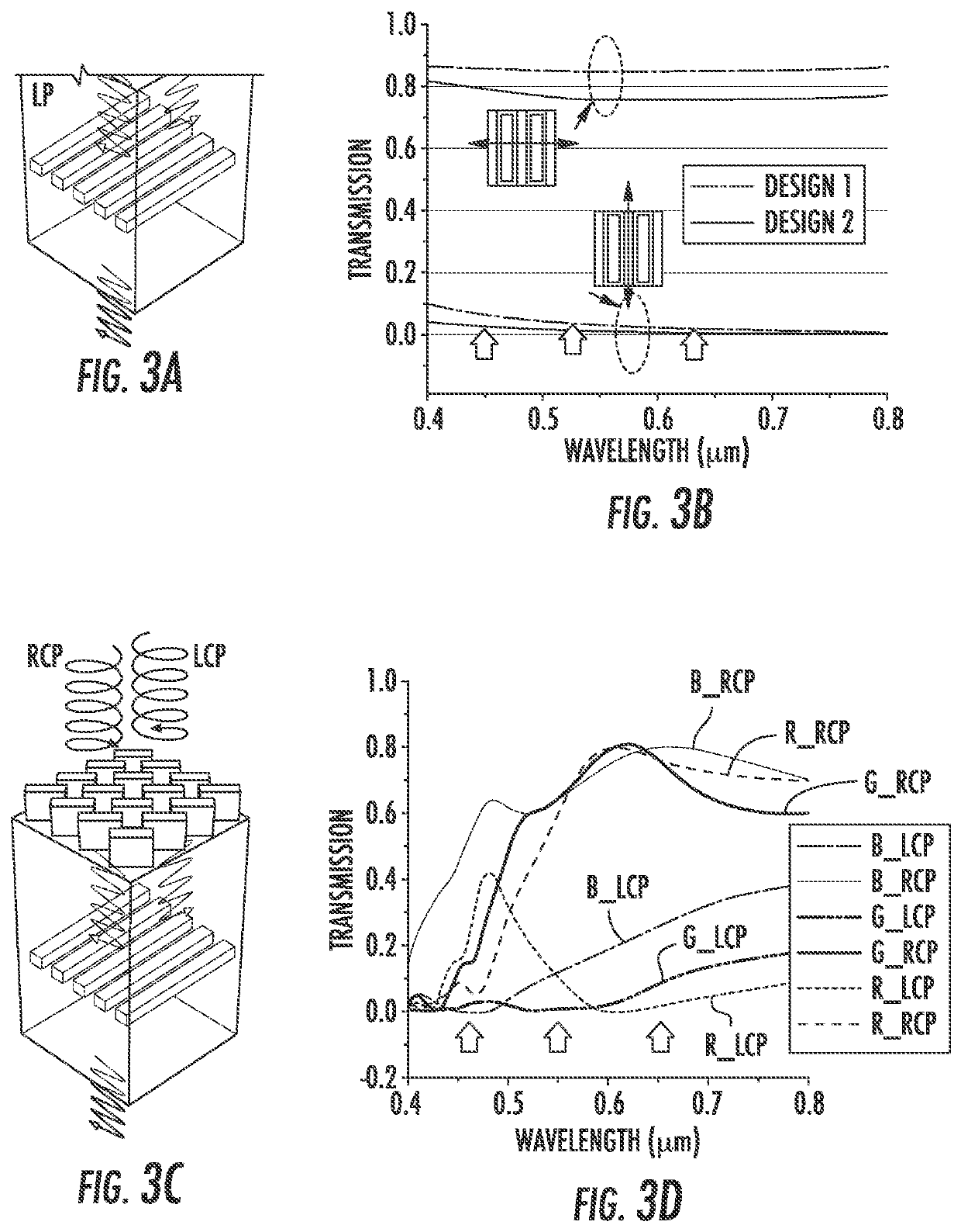
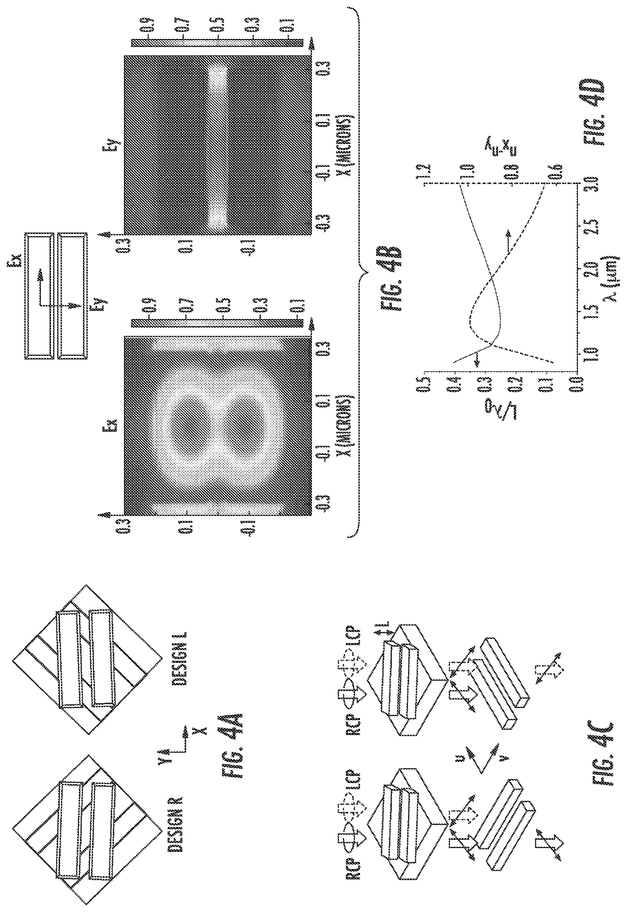
>[0045]Various aspects of the subject technology are now described with reference to the annexed drawings, wherein like reference numerals correspond to similar elements throughout the several views. It should be understood, however, that the drawings and detailed description hereafter relating thereto are not intended to limit the claimed subject matter to the particular form disclosed. Rather, the intention is to cover all modifications, equivalents, and alternatives falling within the spirit and scope of the claimed subject matter.

[0046]As used herein, the singular forms “a”, “an”, and “the” include plural aspects unless the context clearly dictates otherwise.

[0047]This disclosure describes nanoscale optical structures, devices, and methods of making and using the same. It should be apparent to those skilled in the art that many additional modifications beside those already described are possible without departing from the inventive concepts. In interpreting this disclosure, all ...


PUM

PropertyMeasurementUnit
thicknessaaaaaaaaaa
widthaaaaaaaaaa
lengthaaaaaaaaaa

Abstract

A polarization sensor is described. It includes a quarter-wave plate to convert circularly polarized light into linearly polarized light. The quarter-wave plate is realized as a metasurface. The sensor also includes a linear polarizer to analyze the light generated by the quarter-wave plate, and a photodetector to receive the analyzed light. The sensor may be combined with other linear polarization sensors to form a sensor capable of complete measurement of the polarization state of incident light. An array of these sensors can be integrated directly onto image sensors to form a polarimetric imager.

Description

CROSS REFERENCE TO RELATED APPLICATIONS[0001]This application claims priority to U.S. Provisional Patent Application 62 / 609,877, filed on Dec. 22, 2017, which is incorporated herein by reference in its entirety.STATEMENT REGARDING FEDERALLY SPONSORED RESEARCH[0002]This invention was made with government support under 1809997 awarded by the National Science Foundation and under FA9550-16-1-0183 awarded by the Air Force Office of Scientific Research. The government has certain rights in the invention.TECHNICAL FIELD[0003]This application relates to polarization sensing and polarimetric imaging, and in particular, to polarization sensitive optical detectors incorporating polarization sensitive nano-scale metasurfaces.BACKGROUND[0004]The polarization state of a light wave is defined by the oscillation behavior of its associated electric field vector. Light waves may be linearly polarized, indicating a constant orientation of the electric field vector, circularly or elliptically polarize...

Claims


Application Information

Patent Timeline
Patent Type & Authority Applications(United States)
IPC IPC(8): G01J4/04G02B5/30
CPCG01J4/04G02B5/3025G02B1/002B82Y20/00G02B5/3058G02B5/3083G02B27/286
Inventor YAO, YUWANG, CHAOWANG, CHUBAI, JINGBASIRI, ALICHEN, XIAHUI
Owner ARIZONA STATE UNIVERSITY
Why Eureka
Try Eureka