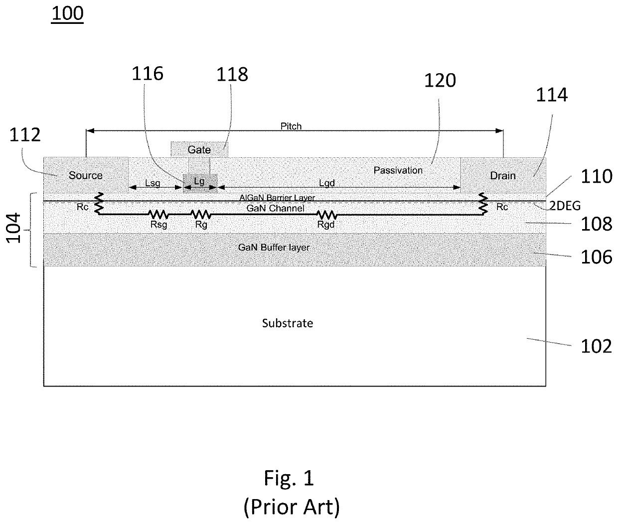
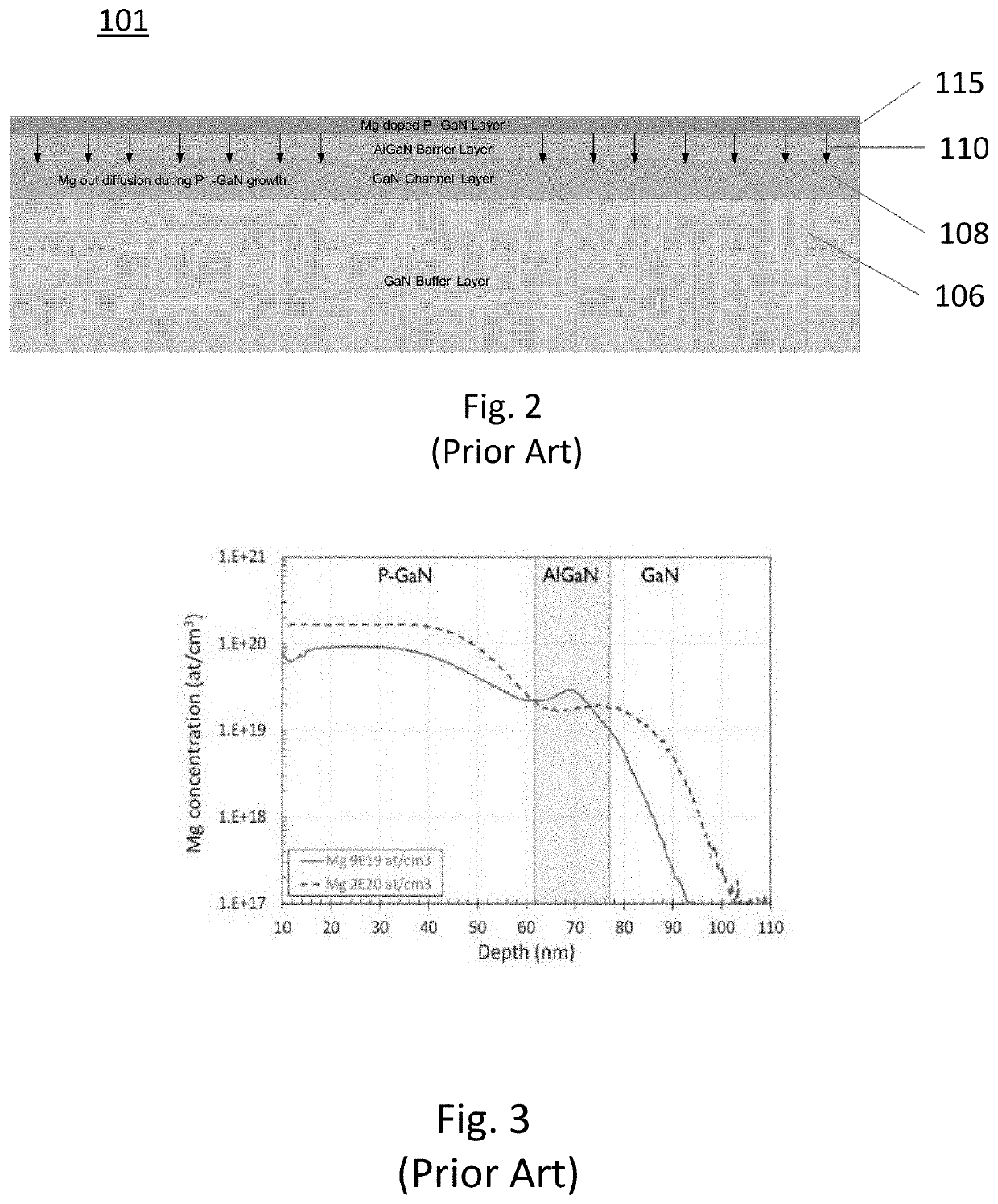
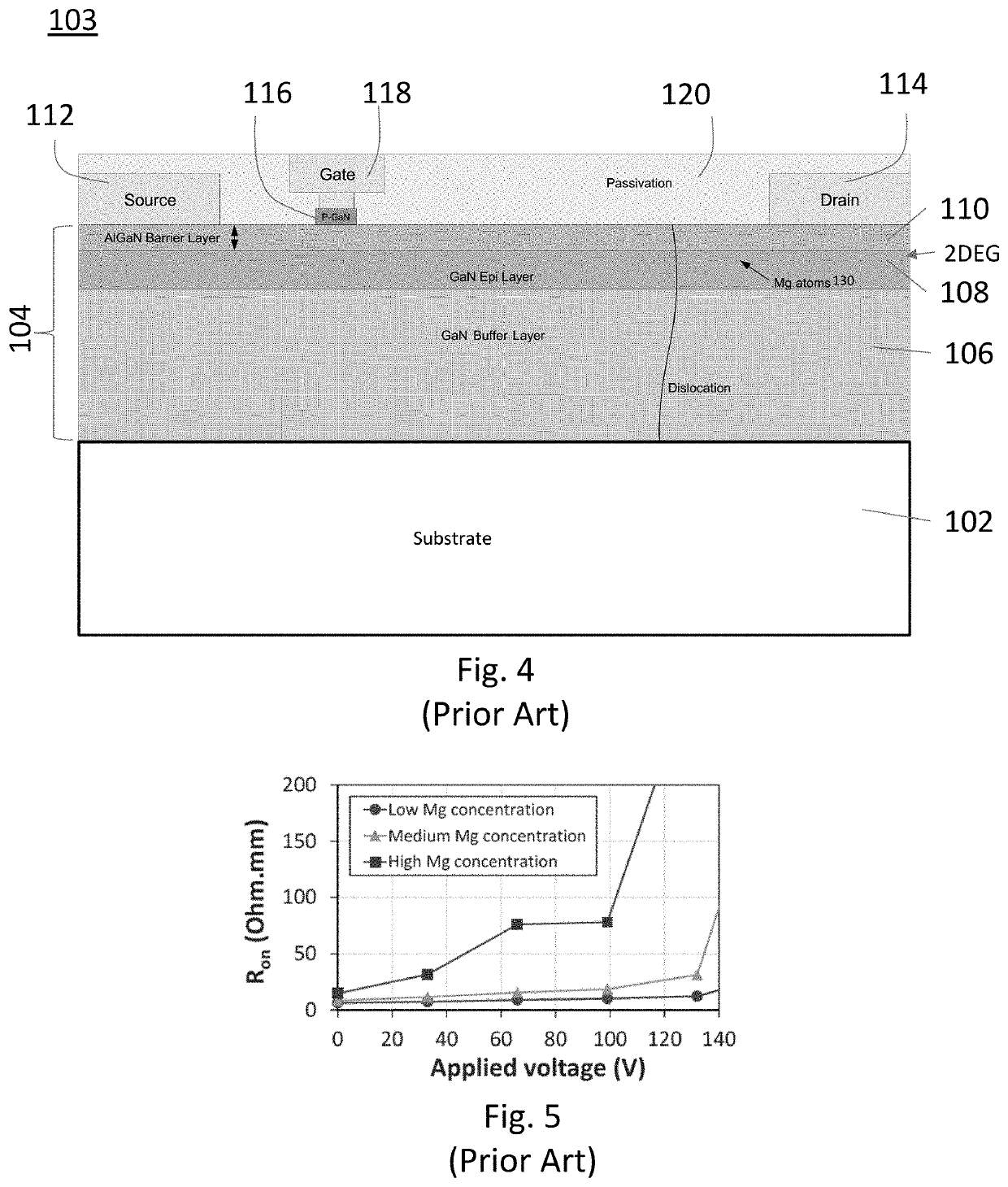
GaN HEMT DEVICE STRUCTURE AND METHOD OF FABRICATION
a technology of gan hemt and device structure, which is applied in the direction of semiconductor devices, basic electric elements, electric apparatus, etc., can solve problems such as depletion mode operation, and achieve the effects of improving device performance, reducing out-diffusion of p-dopants, and improving device performan
- Summary
- Abstract
- Description
- Claims
- Application Information
AI Technical Summary
Benefits of technology
Problems solved by technology
Method used
Image

Examples
first embodiment
[0037]FIGS. 6A, 6B and 6C show schematic cross-sectional views 200-1, 200-2 and 200-3 representing some steps in the method of fabrication of an E-mode GaN HEMT 200, comprising selective gate deposition. This process flow reduces out-diffusion of p-dopant from the p-GaN layer into the underlying layers, to improve device performance. FIG. 6A shows part of the GaN epi-layer stack structure formed on a substrate such as a silicon substrate (not shown) comprising one or more GaN buffer layers 206, and a GaN heterostructure comprising a GaN channel layer 208 and an AlGaN barrier layer 210 forming a 2DEG channel region. As shown in FIG. 6A, after epitaxial growth of the GaN / AlGaN layers of the GaN heterostructure forming the 2DEG channel, a masking layer 220, such as a passivation layer of oxide or nitride is deposited. The masking layer 220 is patterned to define an opening, e.g. a slot 222 in the gate region, exposing the underlying AlGaN barrier layer 210. The gate slot opening 222 i...
third embodiment
[0053]FIGS. 11A, 11B, 11C and 11D show schematic cross-sectional views of some steps in the method of fabrication of the E-mode GaN HEMT device structure 300 of the Selective area p-GaN gate formation allows for the decoupling of the 2DEG channel concentration and the device threshold voltage. To accomplish this known MOCVD growth techniques are used to grow a nucleation layer and one or more buffer layers 306 as well as the GaN channel layer 308. This is followed by an AlGaN barrier layer 310 comprising first and second thicknesses 310a and 310b with variable Al composition, i.e. an Al % profile that varies with thickness, all illustrated schematically in FIG. 11A. For example, the first AlxGa1-xN thickness 310a, adjacent to the GaN channel layer 308, is formed with a first Al % that is between 15% and 18% and a thickness ranging from 15 nm to 20 nm to set the channel threshold voltage. The second AlxGa1-xN thickness 310b has a second Al % that ranges from 20% to 25% with a thickn...
PUM
| Property | Measurement | Unit |
|---|---|---|
| thickness | aaaaa | aaaaa |
| thickness | aaaaa | aaaaa |
| threshold voltage | aaaaa | aaaaa |
Abstract
Description
Claims
Application Information