
Method to print organic electronics without changing its properties

a printing method and electronic technology, applied in printing, semiconductor devices, electrical equipment, etc., can solve the problems of increasing processing time and increasing the number of printing tools required for different materials, and challenging the deposition of organic conducting polymers in a high throughput fashion. , to achieve the effect of efficient us

Pending Publication Date: 2021-08-19
UNIVERSITIES SPACE RES ASSOC
View PDF2 Cites 0 Cited by
  • Summary
  • Abstract
  • Description
  • Claims
  • Application Information

AI Technical Summary

Benefits of technology

This patent describes a method for printing organic electronic materials using a plasma jet. The plasma can either polymerize the materials or break the bonds crucial for electronic conductivity and optimal device performance. The method uses after-glow of the plasma discharge to propel the material towards the substrate and prevent the aerosol containing the materials from getting directly exposed to the plasma region. The nozzle design contains both plasma jet and an aerosol of organic electronic materials separated by a dielectric material that protects the materials in the aerosol from high energy plasma species. This technique prevents potential changes in the chemical structure of the organics and increases the throughput of the printing.

Problems solved by technology

Deposition of organic conducting polymers, small molecules, dendrimers, fluorescent and phosphorescent molecules in a high throughput fashion is challenging as it is absolutely essential to retain the chemical structure and bonding environment of the materials upon printing.
Any change in the chemical bonding and or chemical structure will result in poor performance behavior with deteriorated conducting characteristics.
This also means increased processing time and increased number of printing tools required for different materials.
However, the method described in the literatures will change the properties of the materials as the aerosol containing electronic materials enters the plasma region due to the presence of high energy ions, radicals and electrons in the plasma region.

Method used


Image

  • Method to print organic electronics without changing its properties
  • Method to print organic electronics without changing its properties

Examples


Embodiment Construction

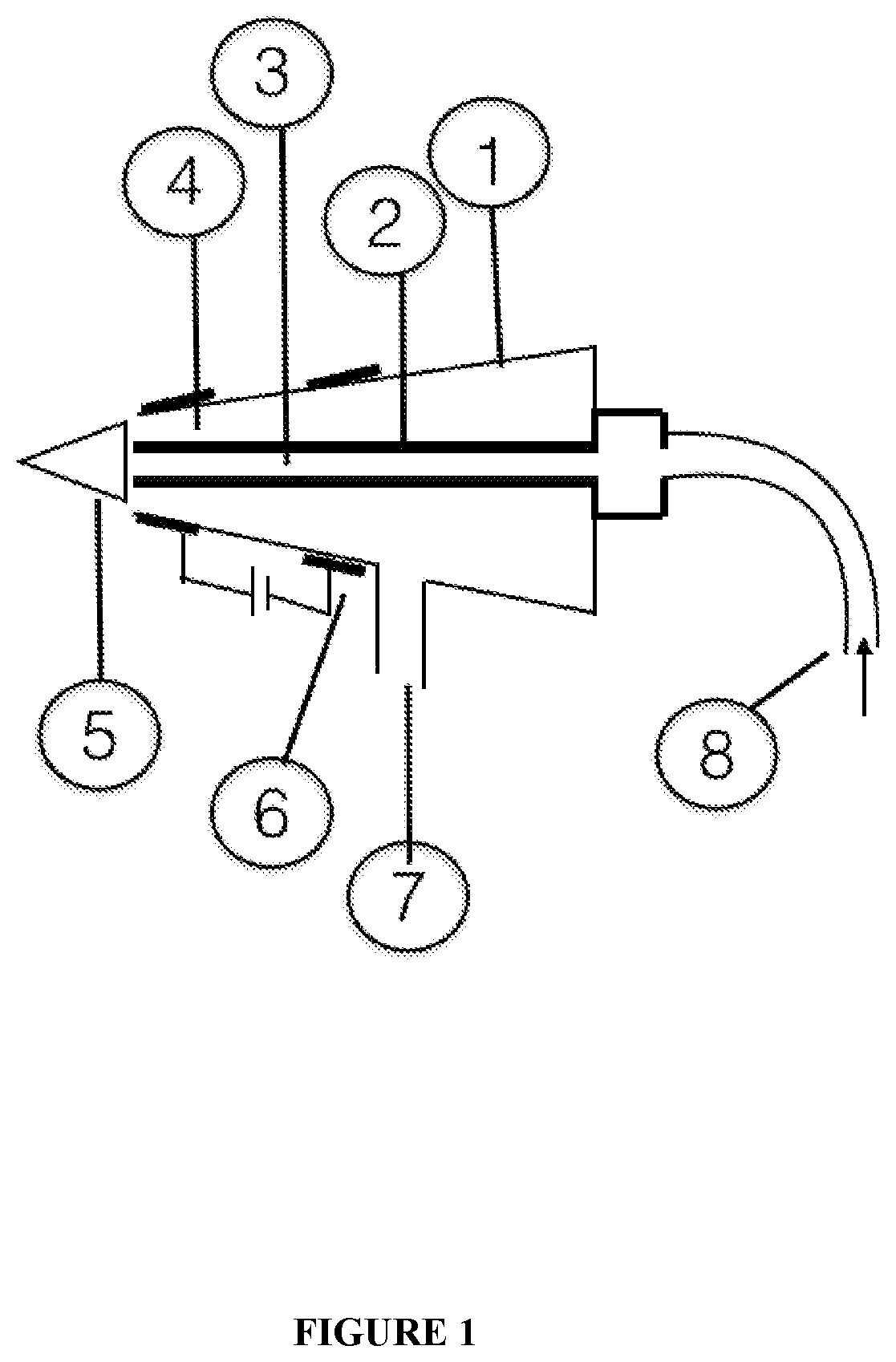
[0044]FIG. 1 shows the schematic of the plasma jet printer nozzle for high throughput direct write printing of organic electronic materials using the after-glow region of the atmospheric pressure plasma and shielding of the aerosol containing organic electronics from the high energy plasma species generated in the dielectric barrier discharge. Various process gases including helium, argon, hydrogen, nitrogen, carbon dioxide, oxygen, methane, alkane, alkene, silane, carbon tetra fluoride, sulfur hexafluoride, etc., can be used on their own or with appropriate mixture to suit the need and depending on the suspension of the organic electronic material.

[0045]FIG. 1 shows the following elements:

[0046]Non concentric conical shaped outer tube 1 with a specific dielectric constant and a specific wall thickness, with a narrow end at the outlet of the nozzle;

[0047]Inner tube 2 with a dielectric constant and / or wall thickness higher than that of tube one;

[0048]Inner region 3 of the inner tube ...


PUM

PropertyMeasurementUnit
diameteraaaaaaaaaa
angleaaaaaaaaaa
angleaaaaaaaaaa

Abstract

Method for high throughput, highly reproducible, direct write plasma jet deposition of organic electronic materials through nozzles containing non-concentric tubes with inner tube having higher dielectric constant and / or higher wall thickness than the outer tube, so that the inner tube containing the aerosol of organic electronic materials is shielded from the outer tube containing plasma and the organic electronics is focused at the outlet of the nozzle through the after-glow region of the atmospheric pressure plasma. Ensuring reproducibility of the method for printing organic electronic materials by removing the contaminants and residues in inner tube using reactive gas and generating a plasma discharge at a potential significantly higher than the operating potential for printing so that the plasma is generated in both the inner and outer tube for dielectric barrier discharge plasma jet based cleaning of the nozzle.

Description

BACKGROUND OF THE INVENTIONField of the Invention[0001]This invention relates to the high throughput direct write printing of conducting electronic materials, using the after-glow region of the atmospheric pressure dielectric barrier discharge plasma jet, without changing the material properties and chemical structure upon printing.Description of the Background[0002]With the development of organic electronic materials, there is a need for developing high throughput printing technology to meet the growing needs for fabrication of organic light emitting diodes, organic photovoltaics, electronic papers, wearable electronics, touch panels, flexible displays and sensors.[0003]Deposition of organic conducting polymers, small molecules, dendrimers, fluorescent and phosphorescent molecules in a high throughput fashion is challenging as it is absolutely essential to retain the chemical structure and bonding environment of the materials upon printing.[0004]Any change in the chemical bonding a...

Claims


Application Information

Patent Timeline
Patent Type & Authority Applications(United States)
IPC IPC(8): H01L51/00B41J2/00H10K99/00
CPCH01L51/0004B41J2/00H01L51/0022H10K71/13H10K71/611
Inventor GANDHIRAMAN, RAMPRASAD
Owner UNIVERSITIES SPACE RES ASSOC
Features
  • Generate Ideas
  • Intellectual Property
  • Life Sciences
  • Materials
  • Tech Scout
  • Unparalleled Data Quality
  • Higher Quality Content
  • 60% Fewer Hallucinations
Learn More