Unlock instant, AI-driven research and patent intelligence for your innovation.

Piezoelectric MEMS Resonators based on Porous Silicon Technologies

a technology of porous silicon and resonators, applied in the direction of electrical equipment, impedence networks, etc., can solve the problems of reducing the performance of resonators based on quartz, not being able to be easily miniaturized for on-chip use, and having some limitations

Active Publication Date: 2021-12-30
TU XIANG ZHENG
View PDF0 Cites 0 Cited by
  • Summary
  • Abstract
  • Description
  • Claims
  • Application Information

AI Technical Summary

Benefits of technology

The present invention provides a piezoelectric MEMS resonator that can be integrated with a CMOS IC in a same silicon substrate using porous-silicon based surface micromachining technology. The resonator has a single crystal silicon microstructure arranged in a selected region of the silicon substrate or a single crystal silicon epitaxial layer grown on a porous silicon layer. It also has a buried cavity with a gap to prevent damage to the suspended microstructure and a post-release process for suspending the microstructure over the cavity. The technical effects of the invention include improved performance and reliability of the piezoelectric MEMS resonator and reduced fabrication costs.

Problems solved by technology

But, resonators based on quartz do have some limitations.
These can not be miniaturized easily for on-chip usage, involves a costly manufacturing process, and their performance degrades when subjected to severe levels of shock and vibration.
Again, the on-chip tank circuits with monolithic inductors and capacitors provided by the present-day integrated circuit technology suffer from poor Q-values.
The main limitation with capacitive resonators is that the capacitive transduction mechanism is employed to excite the resonance mode of a micromechanical structure and also to detect the vibration amplitude.
Therefore, in order to realize reasonably small impedances at high frequencies very small gap sizes are required, which are challenging to fabricate.
The main drawbacks of typical SAW devices are their large size and the incompatible substrates for microelectronic integration.
However, obtaining higher Q and multiple dispersed frequency standards on a single substrate is challenging.
Unfortunately, all above-disclosed thin-film piezoelectric-on-substrate resonators were fabricated using bulk micromachining which is incompatible with CMOS processing.
This incompatibility does not allow mechanical devices to be built at the same time as the electronic logic circuits.
Also, the cost of fabrication is generally higher since this technology can not be run using the same equipment as the semiconductor industry.
Furthermore, the disclosed thin-film piezoelectric-on-substrate resonators were fabricated each using a SOI wafer with a certain thickness of the top silicon layer and a certain thickness of the buried silicon dioxide layer which is not suitable for the design of various purpose thin-film piezoelectric-on-substrate resonators.
Since the released thin silicon MEMS structure is fragile these fabrication steps must become a huge challenge.

Method used


Image

  • Piezoelectric MEMS Resonators based on Porous Silicon Technologies
  • Piezoelectric MEMS Resonators based on Porous Silicon Technologies
  • Piezoelectric MEMS Resonators based on Porous Silicon Technologies

Examples


Embodiment Construction

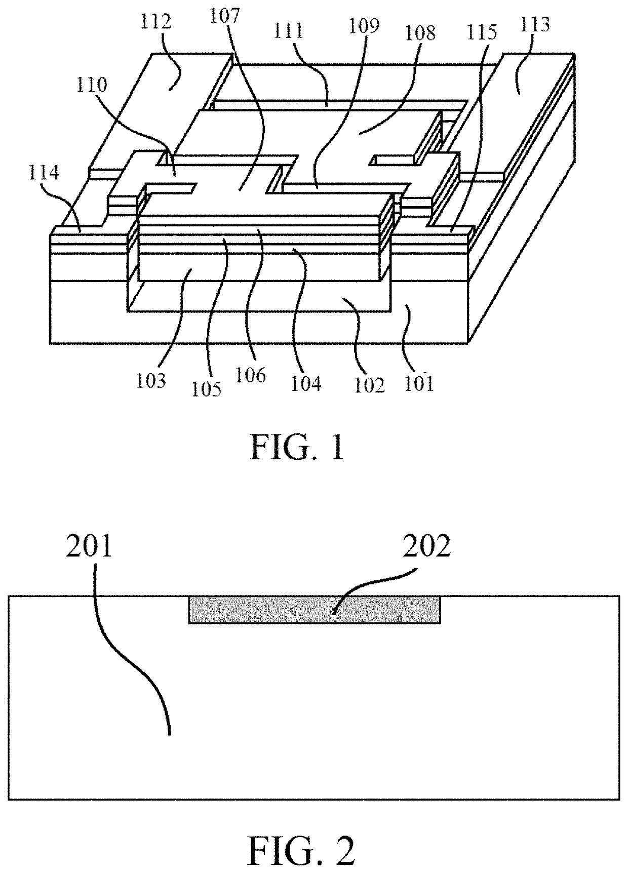
[0039]Radio frequency (RF) communication circuits like reference oscillators, filters, and mixers based on such micro-electro-mechanical system (MEMS) resonators can be utilized for meeting the increasing count of RF components likely to be demanded by the next-generation multi-band / multi-mode wireless devices. MEMS based on-chip resonators have shown significant potential for sensing and high frequency signal processing applications. This is due to their excellent features like small size, large frequency-quality factor product, low power consumption, low cost batch fabrication, and integrability with complementary Metal-Oxide Semiconductor integrated circuit (CMOS IC) technology.

[0040]The utilization of the conventional CMOS IC technology as a platform for design and fabrication of the fast-growing RF MEMS devices has led to development of porous silicon related MEMS technologies. The porous silicon related MEMS technologies include selective formation and etching of porous silico...


PUM


Abstract

A piezoelectric MEMS resonator is provided. The resonator comprises a single crystal silicon microstructure suspended over a buried cavity created in a silicon substrate and a piezoelectric resonance structure located on the microstructure. The resonator is designed and fabricated based on porous silicon related technologies including selective formation and etching of porous silicon in silicon substrate, porous silicon as scarified material for surface micromachining and porous silicon as substrate for single crystal silicon epitaxial growth. All these porous silicon related technologies are compatible with CMOS technologies and can be conducted in a standard CMOS technologies platform.

Description

FIELD OF THE INVENTION[0001]The present invention relates generally to a piezoelectric MEMS resonator and more particularly to a piezoelectric MEMS resonator designed and fabricated based on porous silicon related technologies.BACKGROUND[0002]Resonators can be used to either generate waves of specific frequencies such as oscillators or to select specific frequencies from a signal such as filters. Wireless communications enable resonators to have a wide variety of applications, such as satellite transmission, radio and television broadcasting, sensor networks, global positioning system (GPS), and mobile communications which provide us with voice, data and broadband communication.[0003]A ubiquitous component in modern integrated electronic systems is a frequency-reference circuit. Piezoelectric quartz crystals offering a large quality factor superior frequency temperature stability reliability, technical maturity, and extensive commercial availability are presently in high demand for ...

Claims


Application Information

Patent Timeline
IPC IPC(8): H03H9/17H03H3/02H03H9/02H03H9/13
CPCH03H9/173H03H3/02H03H2009/155H03H9/13H03H9/176H03H9/02031H03H2009/02496H03H9/2405H03H3/0072H03H2003/027H03H2003/021
Inventor TU, XIANG ZHENG
Owner TU XIANG ZHENG