
Polycrystalline Silicon Material

Pending Publication Date: 2022-06-30
TOKUYAMA CORP
View PDF0 Cites 0 Cited by
  • Summary
  • Abstract
  • Description
  • Claims
  • Application Information

AI Technical Summary

Benefits of technology

The present invention provides a way to make a type of silicon that doesn't need a dopant to have high resistivity. This helps in making silicon single crystals with the desired properties.

Problems solved by technology

However, it is difficult to produce a large-diameter ingot by the FZ method, which is disadvantageous in terms of cost.
However, a surface of the polycrystalline silicon material is usually contaminated, and various impurity elements are present on the surface.
Furthermore, a size of the polycrystalline silicon chunk in the polycrystalline silicon material is not constant and has a predetermined particle size distribution.

Method used


Image

  • Polycrystalline Silicon Material

Examples


example 1

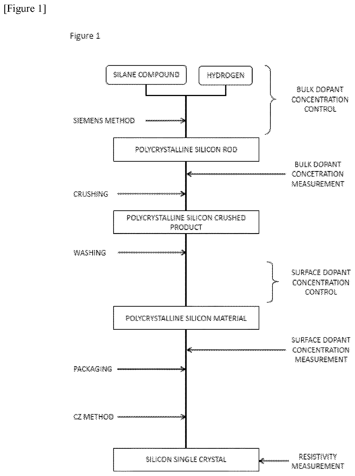
[0137]The polycrystalline silicon material was produced by the Siemens method. As the raw material gas, high-purity purified trichlorosilane and hydrogen were used.

[0138]Purified trichlorosilane produced by the method shown below was used. First, low-purity crude trichlorosilane was obtained by a reaction of metallurgical low-purity silicon called metallic silicon with hydrogen chloride and a reaction of the metallic silicon with tetrachlorosilane and hydrogen.

[0139]B, Al, P, and As were included in the metallic silicon being a raw material of the crude trichlorosilane at ratios of several hundred ppb to several hundred ppm. During the reaction of the metallic silicon with hydrogen chloride and the reaction of the metallic silicon with tetrachlorosilane and hydrogen, each dopant component was chlorinated and get into the crude trichlorosilane.

[0140]Therefore, the obtained crude trichlorosilane was distilled and purified to separate and remove B, P, Al, and As in the crude trichloros...

example 2

[0177]The synthesis, distillation and purification, recovery and purification of trichlorosilane, and the precipitation of polycrystalline silicon were carried out in a similar manner to Example 1. The concentration of dichlorosilane in the recovered purified trichlorosilane in this case was measured by gas chromatography and, as a result, was found to be 600 ppmw.

[0178]The polycrystalline silicon obtained after the precipitation was analyzed by the same method as in Example 1. The average resistivity was 3,100 [Ωcm]. The bulk B concentration was 2 [ppta], and the bulk Al concentration was less than 1 [ppta], which was the lower limit of quantification. The bulk acceptor concentration was set to 2 [ppta], regarding the bulk Al concentration as 0 [ppta]. The bulk P concentration was 31 [ppta] and the bulk As concentration was 2 [ppta]. Therefore, the bulk donor concentration was 33 [ppta].

[0179]Subsequently, in the same manner as in Example 1, the obtained polycrystalline silicon rod...

example 3

[0188]The synthesis, distillation and purification, recovery and purification of trichlorosilane, and the precipitation of polycrystalline silicon were carried out in a similar manner to Example 1. The concentration of dichlorosilane in the recovered purified trichlorosilane in this case was measured by gas chromatography and, as a result, was found to be 350 ppmw.

[0189]The polycrystalline silicon obtained after the precipitation was analyzed by the same method as in Example 1. The average resistivity was 5,300 [Ωcm]. The bulk B concentration was 2 [ppta], and the bulk Al concentration was less than 1 [ppta], which was the lower limit of quantification. The bulk acceptor concentration was set to 2 [ppta], regarding the bulk Al concentration as 0 [ppta]. The bulk P concentration was 17 [ppta] and the bulk As concentration was 2 [ppta]. Therefore, the bulk donor concentration was 19 [ppta].

[0190]Subsequently, in the same manner as in Example 1, the obtained polycrystalline silicon rod...


PUM


Abstract

A polycrystalline silicon material for producing silicon single crystal, containing a plurality of polycrystalline silicon chunks, in which assuming that a total concentration of donor elements present inside a bulk body of the polycrystalline silicon material is Cd1 [ppta], a total concentration of acceptor elements present inside the bulk body of the polycrystalline silicon material is Ca1 [ppta], a total concentration of the donor elements present on a surface of the polycrystalline silicon material is Cd2 [ppta], and a total concentration of the acceptor elements present on the surface of the polycrystalline silicon material is Ca2 [ppta], Cd1, Ca1, Cd2, and Ca2 satisfy a relation of 2 [ppta]≤(Cd1+Cd2)−(Ca1+Ca2)≤8 [ppta].

Description

TECHNICAL FIELD[0001]The present invention relates to a polycrystalline silicon material. In particular, the present invention relates to a polycrystalline silicon material for producing silicon single crystal having a high resistivity.BACKGROUND ART[0002]Silicon single crystal is an extremely important material in industry, and is used as semiconductor wafers, solar cells, radio frequency devices, substrates of various elements such as sensors and the like. When the silicon single crystal is used as the substrate of various elements, the substrate is required to be silicon single crystal having a high resistivity in order to suppress the movement of electric charges in the substrate. For example, as described in Patent Literature 1, a substrate having a resistivity of several thousand Ωcm is required.[0003]The silicon single crystal is obtained as a silicon single crystal ingot by bringing a seed crystal into contact with a silicon melt obtained by melting a polycrystalline silicon...

Claims


Application Information

Patent Timeline
IPC IPC(8): C01B33/035C30B29/06C30B15/36
CPCC01B33/035C01P2006/80C30B15/36C30B29/06C30B15/00C01B33/02
Inventor ASANO, TAKUYASAIKI, KOUICHIEMOTO, MIKIONODA, TOORU
Owner TOKUYAMA CORP
Learn More