Edge emitting laser device

a laser device and laser technology, applied in lasers, laser optical resonator construction, semiconductor lasers, etc., can solve the problems of higher material requirements, more complicated structure of laser devices, and more difficult design, so as to reduce the series resistance of edge emitting laser devices, reduce the resistance of p-type cladding layers, and increase the modal gain

Pending Publication Date: 2022-08-04
ABOCOM SYST
View PDF0 Cites 0 Cited by
  • Summary
  • Abstract
  • Description
  • Claims
  • Application Information

AI Technical Summary

Benefits of technology

[0007]In view of the problems of the prior art, it is a primary objective of the present disclosure to overcome the problems of the prior art by providing an edge emitting laser device. The present disclosure is based on the fact that the resistance of the p-type cladding layer of the edge emitting laser device is much greater than the resistance of the n-type cladding layer of the edge emitting laser device since most of the series resistance of the edge emitting laser device comes from the p-type cladding layer, therefore a part of the p-type cladding layer is converted into the n-type cladding layer to reduce the series resistance of the edge emitting laser device. The present disclosure is also based on the fact that a part of the p-type cladding layer is converted into the n-type cladding layer, such that the coupling of the optical field with the quantum well of the active layer tends to take place at the middle position of the thickness of the active layer, such that the lower half of the active layer can be utilized effectively and can compensate the vertical deviation of the optical field, so as to increase the modal gain and reduce the threshold current value. As a result, the edge emitting laser device can be operated at a high temperature condition and has a high operating speed. The present disclosure is further based on the fact that a part of the p-type cladding layer is converted into the n-type cladding layer, such that the optical field is relatively near the grating layer to achieve a better coupling efficiency of the optical field / grating and a lower threshold current value. As a result, the edge emitting laser device can be operated at the high temperature condition and has a high operating speed.

Problems solved by technology

The LED device is a divergent light source, but its luminous energy is weak and the beam angle is too large, so that its functionality is insufficient and the LED device can only provide general lighting or can be used in 2D sensing systems.
From the aspect of structure, the LD device structure is more complicated, the material requirement is higher, and the design is more difficult than those of the LED device, so that the mass production of the LD devices requires a higher level of difficulty of the epitaxial technology.
However, the concentration for the zinc doping of p-type cladding layer cannot be controlled easily, and if it is necessary to have a p-type cladding layer with a resistance lower than the predetermined resistance value, the doping concentration of zinc is adjusted to over 2.5×10¹⁸ atoms / cm3, but such high doping concentration of zinc will make the epitaxial growth of the p-type cladding layer very difficult, the value of the threshold current (Ith) of the p-type cladding layer unable to be reduced, thereby affecting the electrical property, and the p-type cladding layer absorbing light, or even after the FP laser device and the DFB laser device have been used for a period of time, the too-high concentration zinc in the p-type cladding layer will migrate to the active layer and affect the performance of the active layer.
Therefore, the traditional EEL device has encountered an issue of unable to effectively overcome the high series resistance.
In the structure of the traditional FP laser device and DFB laser device, the electrons coming from the n-type cladding layer and the lower confinement layer at the bottom side of the laser device has a mobility greater than the electron holes coming from the p-type cladding layer and the upper confinement layer at the top side of the laser device, so that most of the electrons and electron holes are actually coupled at the upper half of the active layer to emit light, thereby leading to the fact that the lower half of the active layer cannot be utilized effectively.
In addition, this will make most of the optical field deviates in the upper half of the active layer (also known as the vertical deviation of the optical field), and the coupling of the optical field with the quantum well of the active layer will also deviate in the upper half of the active layer, thereby leading to the facts that the modal gain cannot be increased, the threshold current value cannot be reduced, the high operating speed (such as 10 Gb / s) cannot be achieved, and the operation cannot be performed at high temperature.
When the carrier is injected into the active layer, an overflow is more likely to occur as the temperature rises, which also leads to the reduction of the coupling efficiency of the carrier in the active layer.

Method used


Image

  • Edge emitting laser device
  • Edge emitting laser device
  • Edge emitting laser device

Examples


first embodiment

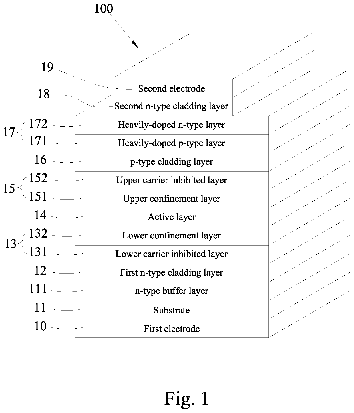
[0034]Table 2 lists the structural comparison of an EEL device (or FP laser device) in accordance with the present disclosure.

TABLE 2(First Embodiment)ThicknessDopant ContentLayerDescriptionMaterial(nm)Dopant(atoms / cm3)Type 1First electrodeInP200S1.0 × 1018~5.0 × 10¹⁸n10 2Substrate 11InP350000S1.0 × 1018~5.0 × 10¹⁸n 3n-type bufferInP500Si1.0 × 1018nlayer 111 4First n-typeInP100Si1.0 × 1018ncladding layer12 5Lower carrierAlInAs140Si5.0 × 1017ninhibited layer131 6LowerAlGaInAs50———confinementlayer 132 7Active layer 14AlGaInAs*Note——— 8UpperAlGaInAs50———confinementlayer 151 9Upper carrierAlInAs50———inhibitor layer15210p-type claddingInP50Zn5.0 × 1017player 1611Tunnel junctionInGaAsP15CGreater thanplayer 171.0 × 10¹⁹(heavily-dopedp-type layer171)Tunnel junctionInGaAsP15TeGreater thannlayer 171.0 × 10¹⁹(heavily-doped n-typelayer 172)12Second n-typeInP1500Si7.0 × 1017~1.5 × 10¹⁸ncladding layer1813SecondInGaAs200TeGreater thannelectrode 191.0 × 10¹⁹*Note:The thickness of the active layer c...

second embodiment

[0038]Table 4 lists the structural comparison of an EEL device (or DFB laser device) in accordance with the present disclosure.

TABLE 4(Second Embodiment)ThicknessDopant ContentLayerDescriptionMaterial(nm)Dopant(atoms / cm3)Type 1First electrodeInP200S1.0 × 1018~5.0 × 10¹⁸n10 2Substrate 11InP350000S1.0 × 1018~5.0 × 10¹⁸n 3n-type bufferInP500Si1.0 × 1018nlayer 111 4First n-typeInP100Si1.0 × 1018ncladding layer124-1Grating layer GInGaAsP35Si1.0 × 1018n4-2Spacer layer SInP150Si1.0 × 1018n 5Lower carrierAlInAs50Si5.0 × 1017ninhibited layer131 6LowerAlGaInAs50———confinementlayer 132 7Active layer 14AlGaInAs*Note——— 8LowerAlGaInAs50———confinementlayer 151 9Upper carrierAlInAs50———inhibited layer15210p-type claddingInP50Zn5.0 × 1017player 1611Tunnel junctionInGaAsP15CGreater thanplayer 171.0 × 10¹⁹(heavily-dopedp-type layer171)Tunnel junctionInGaAsP15TeGreater thannlayer 171.0 × 10¹⁹(heavily-dopedn-type layer172)12Second n-typeInP1500Si7.0 × 1017~1.5 × 10¹⁸ncladding layer1813SecondInGaAs200Te...

third embodiment

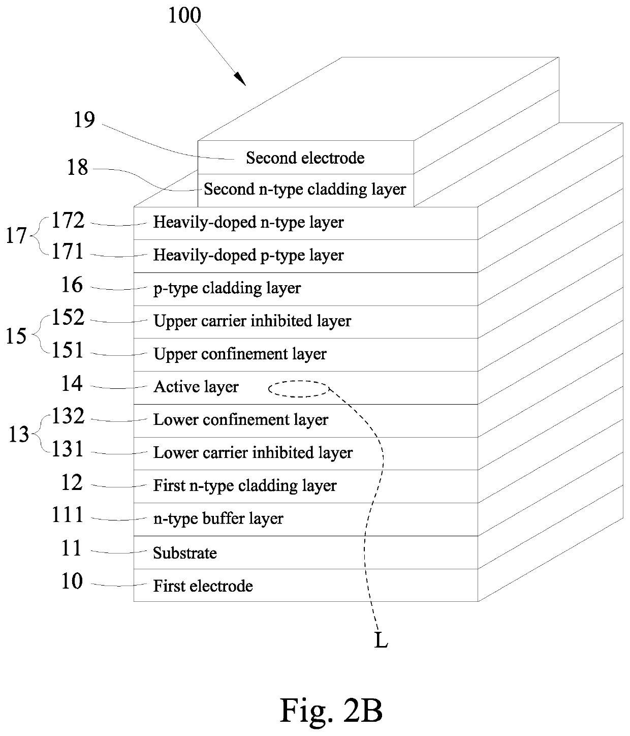
[0042]Table 6 lists the structural comparison of an EEL device (or DFB laser device) in accordance with the present disclosure.

TABLE 6(Third Embodiment)ThicknessDopant ContentLayerDescriptionMaterial(nm)Dopant(atoms / cm3)Type 1First electrode 10InP200S1.0 × 1018~5.0 × 10¹⁸n 2Substrate 11InP350000S1.0 × 1018~5.0 × 10¹⁸n 3n-type buffer layerInP500Si1.0 × 1018n111 4First n-typeInP100Si1.0 × 1018ncladding layer 12 5lower carrierAlInAs50Si5.0 × 1017ninhibited layer 131 6LowerAlGaInAs50———confinement layer132 7Active layer 14AlGaInAs*Note——— 8UpperAlGaInAs50———confinement layer151 9Upper carrierAlInAs50———inhibited layer 15210p-type claddingInP20Zn5.0 × 1017player 1611Tunnel junctionInGaAsP15CGreater thanplayer 171.0 × 10¹⁹(heavily-doped p-type layer 171)Tunnel junctionInGaAsP15TeGreater thannlayer 17 (heavily-1.0 × 10¹⁹doped n-type layer172)12Lower second n-InP25Si1.0 × 1018ntype claddinglayer 18112-1Grating layer GInGaAsP15Si1.0 × 1018n13Upper second n-InP1500Si7.0 × 1017~1.5 × 10¹⁸ntype...


PUM

PropertyMeasurementUnit
thicknessaaaaaaaaaa
thicknessaaaaaaaaaa
thicknessaaaaaaaaaa

Abstract

An edge emitting laser (EEL) device includes a substrate, an n-type buffer layer, a first n-type cladding layer, a grating layer, a spacer layer, a lower confinement unit, an active layer, an upper confinement unit, a p-type cladding layer, a tunnel junction layer and a second n-type cladding layer sequentially arranged from bottom to top. The tunnel junction layer can stop an etching process from continuing to form the second n-type cladding layer into a predetermined ridge structure and converting a part of the p-type cladding layer into the n-type cladding layer to reduce series resistance of the EEL device. Therefore, the optical field and active layer tend to be coupled at the middle of the active layer, the lower half of the active layer can be utilized effectively, and the optical field is near to the grating layer to achieve better optical field / grating coupling efficiency and lower threshold current.

Description

CROSS-REFERENCE TO RELATED APPLICATIONS[0001]This non-provisional application claims priority under 35 U.S.C. § 119(a) on Patent Application No(s). 110103352 filed in Taiwan, R.O.C. on Jan. 29, 2021, the entire contents of which are hereby incorporated by reference.BACKGROUNDTechnical Field[0002]The present disclosure relates to an edge emitting laser (EEL) device, and more particularly to a Fabry-Perot (FP) laser device, a distributed feedback (DFB) laser device, and a laser device with a ridge waveguide structure.Description of Related Art[0003]Semiconductor light emitting device can be divided into light emitting diode (LED) device and laser diode (LD) device. The LED device is a divergent light source, but its luminous energy is weak and the beam angle is too large, so that its functionality is insufficient and the LED device can only provide general lighting or can be used in 2D sensing systems. On the other hand, the LD device generates laser light with a beam angle and a shap...

Claims


Application Information

Patent Timeline
Patent Type & Authority Applications(United States)
IPC IPC(8): H01S5/20H01S5/34H01S5/12H01S5/30
CPCH01S5/20H01S5/3416H01S5/343H01S5/3077H01S5/12H01S5/3095H01S5/2009H01S5/2004H01S5/22H01S5/3213H01S5/3235H01S5/305H01S5/3054
Inventor OU, CHENG-YILIN, CHIH-YUANCHI, CHENG-HSIAO
Owner ABOCOM SYST
Why Eureka
Try Eureka