

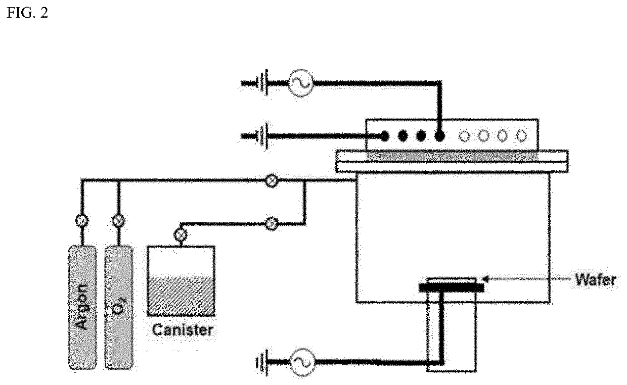
Plasma etching method
a technology of etching method and plasma, which is applied in the field of etching method, can solve the problems of lowering the etching rate, the method has fundamental limits, and the etching is not performed to achieve the desired etching depth, etc., and achieves excellent etching characteristics, reduce greenhouse gas emission, and increase the etching rate
- Summary
- Abstract
- Description
- Claims
- Application Information
AI Technical Summary
Benefits of technology
Problems solved by technology
Method used
Image

Examples
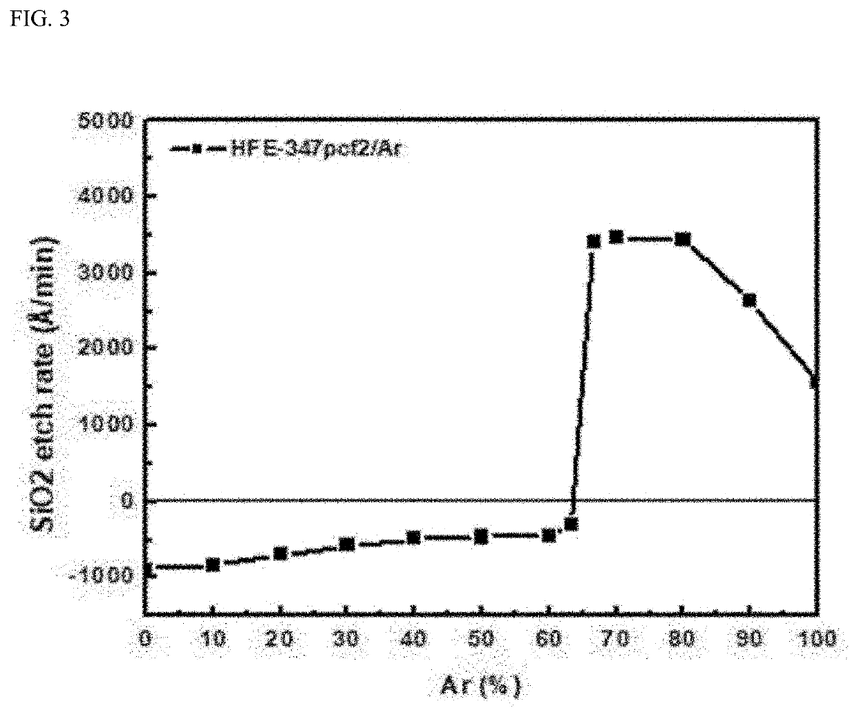
experimental example 4
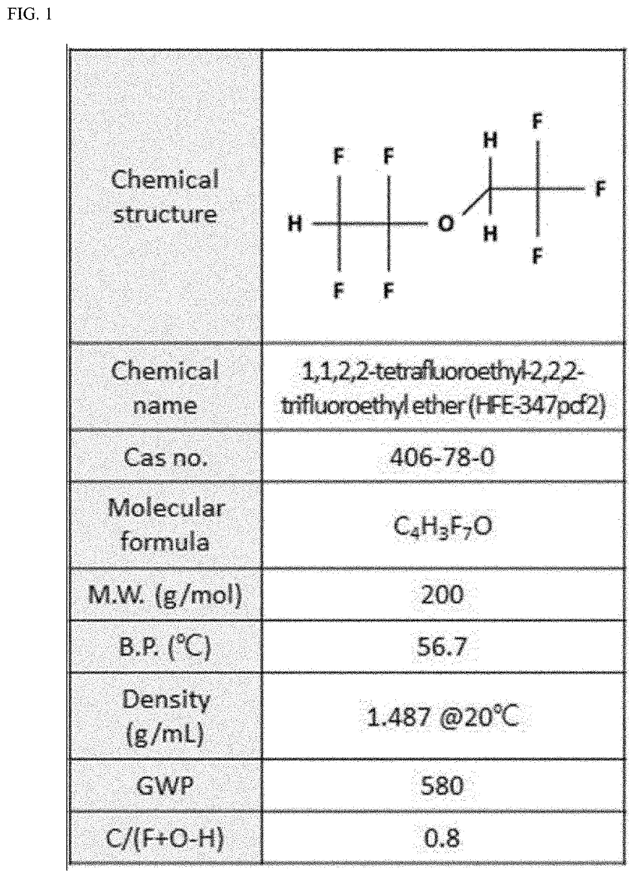
HFE-347pcf2 / Ar and HFE-347pcf2 / Ar / O2
[0049]In order to manufacture a high-aspect-ratio etched structure via the etching process using the HFE-347 / Ar plasma according to the present disclosure, first, a hole pattern mask was formed on a specimen (SiO2 thin film). The formed hole pattern mask was imaged using FE-SEM, and the result is shown in FIG. 8.
[0050]Referring to FIG. 8, it may be identified that the hole pattern mask has a total thickness of 1400 nm, and has a structure in which a 50 nm SiON thin film is present on 1350 nm ACL, and is formed on a 2400 nm SiO2 thin film. Further, it may be identified that a diameter of the formed hole pattern mask is 200 nm.
[0051]High aspect ratio etching of the specimen (SiO2 thin film) on which the hole pattern mask prepared as described above is formed using each of HFE-347pcf2 / Ar plasma and HFE-347pcf2 / Ar / O2 plasma was identified. Specifically, plasma etching was performed under conditions of following table 4. The result is shown in FIG. 9....
PUM
| Property | Measurement | Unit |
|---|---|---|
| GWP | aaaaa | aaaaa |
| diameter | aaaaa | aaaaa |
| boiling point | aaaaa | aaaaa |
Abstract
Description
Claims
Application Information