GaN based optoelectronic device and method for manufacturing the same

a technology of optoelectronic devices and gans, which is applied in the direction of semiconductor devices, lasers, semiconductor lasers, etc., can solve the problems of difficult to grow bulk single crystals, difficult to control stoichiometry, and general difficulty in controlling hole concentrations in p-type semiconductor regions

Inactive Publication Date: 2000-02-01
KK TOSHIBA
View PDF3 Cites 66 Cited by
  • Summary
  • Abstract
  • Description
  • Claims
  • Application Information

AI Technical Summary

Problems solved by technology

However, GaN has a rather high melting point of 1700.degree. C. or higher as well as an extremely high equilibrium vapor pressure of nitrogen at the growth temperature, so that its stoichiometric composition (stoichiometry) is hard to control and therefore is difficult to grow bulk single-crystals.
The hole concentrations in the p-type semiconductor regions, however, are generally hard to control and concerted efforts were made to dope GaN based semiconductor p-type.
That is, one known problem is that in the growth of a Mg-doped GaN layer by the MOCVD method etc., when the substrate temperature is lowered down to the room temperature (during which an NH.sub.3 gas generally continues to be supplied as a source of the column V element to avoid dissociation of N from the surface of the growth layer), the growth layer incorporates atomic H, which passivate the acceptors, thus providing a high resistivity of the Mg-doped GaN layer.
These methods, however, suffer in a respect that a complicated process of electron-beam irradiation or th

Method used


Image

  • GaN based optoelectronic device and method for manufacturing the same
  • GaN based optoelectronic device and method for manufacturing the same
  • GaN based optoelectronic device and method for manufacturing the same

Examples


first embodiment

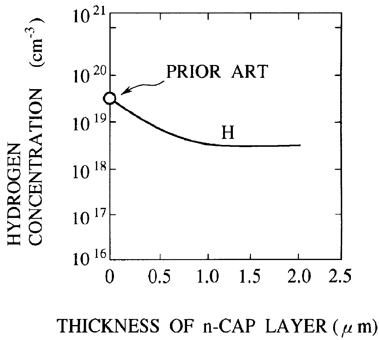
the present invention is not limited to the above-mentioned modifications as well as the structures and methods for manufacturing the same. That is, it can be applied also to more general GaN based LEDs, semiconductor lasers and photodetectors having In.sub.x Al.sub.y Ga.sub.1-x-y N layers. Although the n-cap layers made of GaN or InAlGaN have been described above, almost the same effectiveness can be obtained also with other semiconductor materials as far as their electrical characteristics are of an n type. A variety of other modifications are possible without departing from the spirit and the scope of the present invention.

[Second Embodiment]

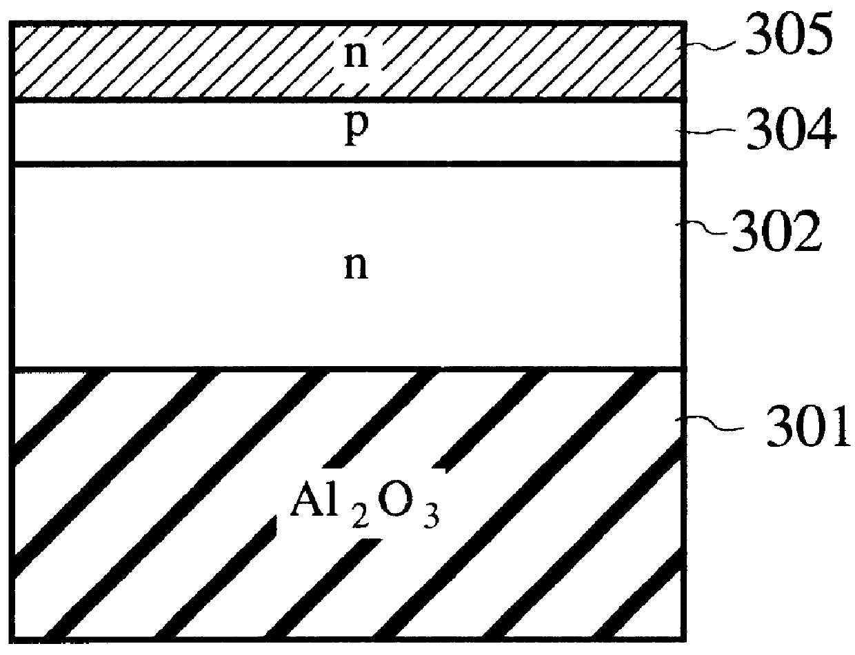
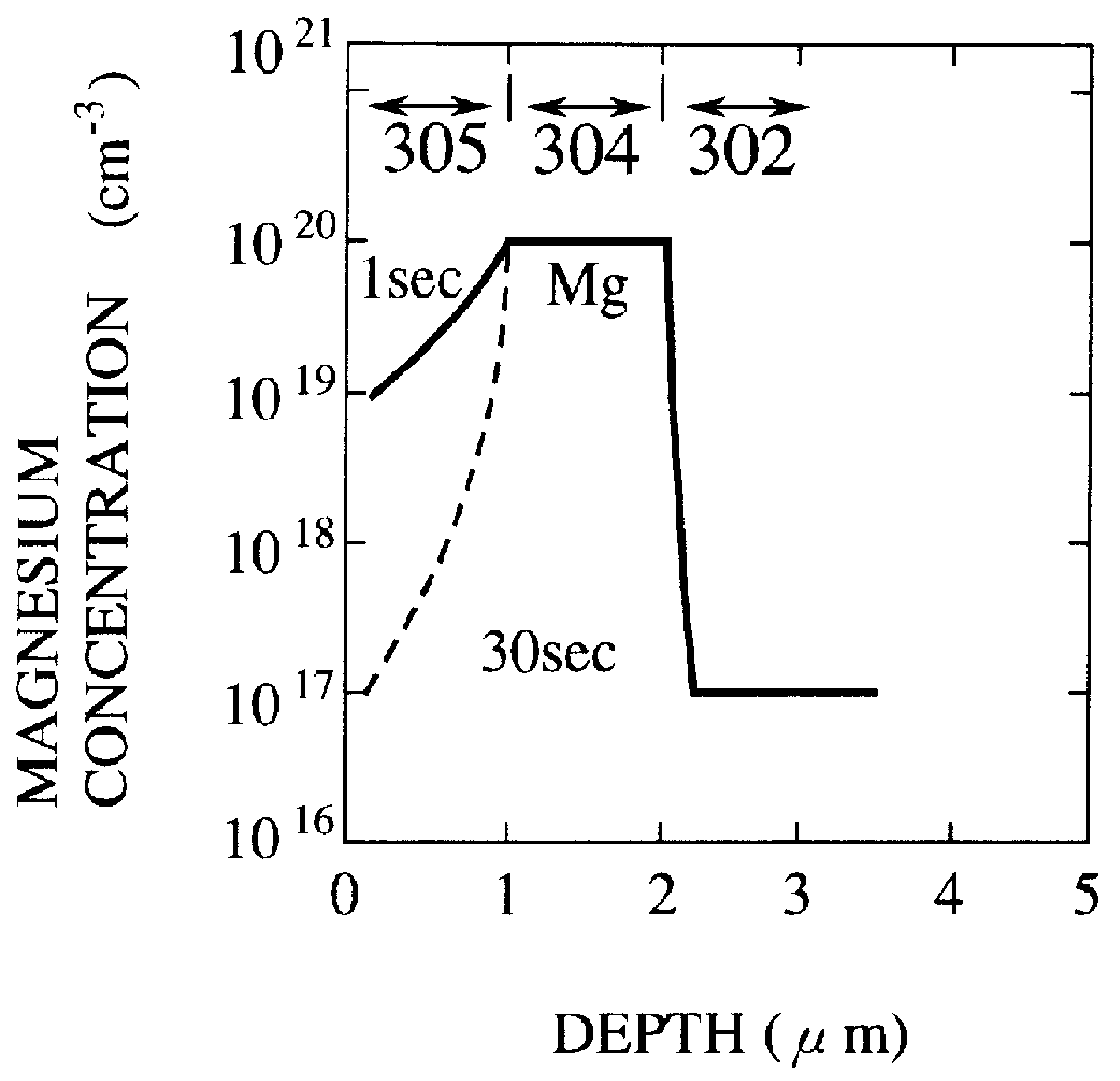
FIG. 7A is a cross-sectional view of a stacked structure of a GaN based optoelectronic device related to the second embodiment of the present invention. As shown in it, on a main surface of a sapphire (Al.sub.2 O.sub.3) substrate 301 are consecutively stacked a Si-doped n-type GaN layer 302 and a Mg-doped p-type GaN layer 314 in this order. T...

second embodiment

the present invention is not limited to the structure shown in FIGS. 7A and 7B. Although the GaN layer 315 has been used as the n-cap layer in FIG. 7B, any other semiconductor materials such as the above-mentioned n-type InAlGaN etc. are adaptable to the n-cap layer providing the same effects, as far as their electrical characteristics are of an n type. Also, although the second embodiment of the present invention can be applied not only to light-emitting diodes but also to other optoelectronic devices such as semiconductor lasers and photodetectors. Although a N.sub.2 gas and a N.sub.2 -rich mixed gas of H.sub.2 / N.sub.2 have been used as an atmospheric gas at time of temperature lowering, the same effects can be obtained also with an inert gas such as Ar, He, etc. or their mixed gas. A variety of other modifications are possible without departing from the spirit and the scope of the present invention.

[Third Embodiment]

FIG. 8A is a cross-sectional view of a stacked structure of a G...

third embodiment

the present invention is not limited to such a structure as shown in FIGS. 8A and 8B. It is of course possible, like in the case shown in FIG. 3A, to form the n-type In.sub.x Al.sub.y Ga.sub.1-x-y N buffer layer and the undoped (or n.sup.- -type) GaN layer on the sapphire substrate 301 and then form the n-type GaN layer 302. The present embodiment can be applied also to DH light-emitting diodes and semiconductor lasers and other optoelectronic devices such as photodetectors without departing the spirit and the scope of the present invention.

Various modifications will become possible for those skilled in the art after receiving the teachings of the present disclosure without departing from the scope of thereof.


PUM


Abstract

An n-cap layer is formed on a top surface of p-type clad layers, the p-type clad layer is a top layer of a stacked structure having a pn-junction for emitting carriers into light-emitting region of a GaN based light-emitting device, thus increasing the activation ratio of acceptor impurities in the p-type clad layers. The n-cap layer is used also as a current blocking layer, thereby constructing a current-blocked structure. The n-cap layer should preferably be made of InuAlvGa1-u-vN (0<u, v<1) deposited as thick as 1.0 micron or more. The present invention will easily provide a high luminous efficiency GaN based semiconductor light-emitting device without using any complicated processes such as electron-beam irradiation or thermal annealing.

Description

1. Field of the InventionThe present invention relates in general to optoelectronic devices (such as light-emitting diodes (LEDs) or semiconductor lasers made of compound semiconductor materials) and a method for manufacturing the devices. More particularly, the present invention relates to semiconductor light-emitting devices made of gallium nitride (GaN) based semiconductor material and a method for manufacturing the same. Such devices are essential for developing full color displays and, in the case of coherent light sources, high density optical storage technologies. Also, the devices are very likely to be used as devices for signal and illumination applications.2. Description of the Prior ArtThe GaN based semiconductors such as In.sub.x Al.sub.y Ga.sub.1-x-y N show high-efficiency radiative recombinations due to their direct transition natures. And, in view of the available wide range of bandgaps from 2.0 eV to 6.2 eV, the GaN based semiconductors have been developed as materia...

Claims


Application Information

Patent Timeline
IPC IPC(8): H01L33/00H01L33/04H01L33/14H01L33/32H01L33/38
CPCH01L33/04H01L33/145H01L33/32H01L33/325H01S5/32H01L33/20H01L33/42
Inventor SUGAWARA, HIDETOISHIKAWA, MASAYUKI
Owner KK TOSHIBA
Why Eureka
Try Eureka