Method for formation of multilayer film

a multi-layer film and film technology, applied in the field of multi-layer film formation, can solve the problems of inferior interfaces going to impair the device characteristics, failure to form highly satisfactory interfaces between the component films of multi-layer films, and failure to form highly satisfactory interfaces between multi-layer films, etc., to achieve the effect of high yield, reduced time spent on the formation of multi-layer films, and high desirable interfaces

Inactive Publication Date: 2000-03-14
JAPAN DISPLAY CENTRAL CO LTD
View PDF9 Cites 86 Cited by
  • Summary
  • Abstract
  • Description
  • Claims
  • Application Information

AI Technical Summary

Benefits of technology

This invention, as described above, concerns a method for forming a multilayer film while continuously retaining a state of plasma without interruption. The state of plasma between the steps for formation of a deposited film can be optimized by adjusting such conditions as the distance between the electrodes, the kinds of gas introduced, the internal pressure of the reaction chamber, and the magnitude of the high-frequency electric power supplied. Thus, a multilayer film of uniform quality can be formed from a stable plasma state. The multilayer film possesses a highly desirable interface because of freedom from blister or separation. The multilayer film is formed in a high yield. Since the state of plasma does not need to be reformed, the time spent for the formation of the multilayer film can be decreased and the efficiency of the production can be improved.
Thus, the TFT to be consequently produced is enabled to acquire outstanding characteristics mainly because the defective density (dangling bond) near the interface between the gate insulating film and the semiconductor film, the interface between the semiconductor film and the etching-stopper-film on channel, and the interface between the semiconductor film and the gate insulating film is decreased.

Problems solved by technology

As described above, the methods heretofore adopted for the formation of a multilayer film are at a disadvantage in failing to form highly satisfactory interfaces between the component films of multilayer films because the plasma state is stopped or because the plasma state, if not stopped, cannot be optimized during the step of film forming.
The fact that no satisfactory interfaces are formed entails the problem that the interfaces are blistered or separated to the extent of degrading the yield of production.
When the multilayer film constitutes itself such a semiconductor device as a TFT, the inferior interfaces go to impair the characteristics of the device.
The time thus spent goes to degrade the efficiency of the production.

Method used


Image

  • Method for formation of multilayer film
  • Method for formation of multilayer film
  • Method for formation of multilayer film

Examples


example 2

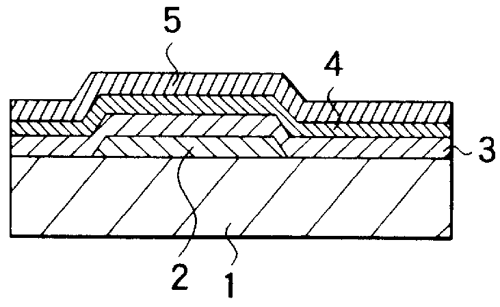
FIG. 4 shows a TFT in an active matrix type liquid crystal display device according to Example 2. This TFT is composed of a gate electrode 2 formed in a predetermined shape of Mo-Ta integrally with a gate line (not shown) on a glass insulating substrate 1, a gate insulating film 3 of SiN.sub.x formed in a thickness of 0.3 .mu.m in such a manner on the insulating substrate 1 as to cover the gate electrode 2, a semiconductor film 4 formed in a predetermined shape of a-Si, microcrystalline silicon, or polycrystalline silicon in a thickness of 0.05 .mu.m in such a manner as to cover the gate insulating film 3 in conformity to the gate electrode 2, an n type semiconductor film 6 formed of n.sup.+ a-Si in such a manner as to cover the source region and the drain region other than the channel region on the semiconductor film 4, a source electrode 7 formed on the n type semiconductor film 6 as partly extended into the source region on the gate insulating film 3, a drain electrode 8 formed l...

example 3

FIG. 6 shows a normal staggered (top-gate) TFT according to Example 3. In this TFT, an insulating substrate 1 made of glass (such as, for example, a product of Corning Glass marketed under product code of "7059") is heated to 623K and a gas composed of SiH.sub.4 and nitrogen suboxide (N.sub.2 O) is introduced and, by the plasma CVD technique using the plasma state which is consequently generated, an undercoat film 21 of SiO.sub.2 is deposited in a thickness of 0.5 .mu.m.

Then, an ITO film of a thickness of 0.1 .mu.m for the formation of a pixel electrode 10 is formed and a metal of Mo-W is deposited in the form of a film by the sputtering technique. These films are photolithographically etched to form a source electrode 7 and a drain electrode 8 in predetermined shapes.

Then, the insulating substrate 1 is heated to 623K and the material gas for the deposition of a semiconductor layer which is composed of SiH.sub.4 and H.sub.2 is introduced to generate a plasma state and deposit an a-S...

example 4

The construction of a liquid crystal display device (LCD) using the aforementioned TFT as a switching element is shown in FIG. 7. This liquid crystal display device is composed of an active element substrate 26, a counter substrate 27 opposed to the active element substrate 26 across a predetermined interval, and a liquid crystal 28 filling the gap between these substrates 26 and 27.

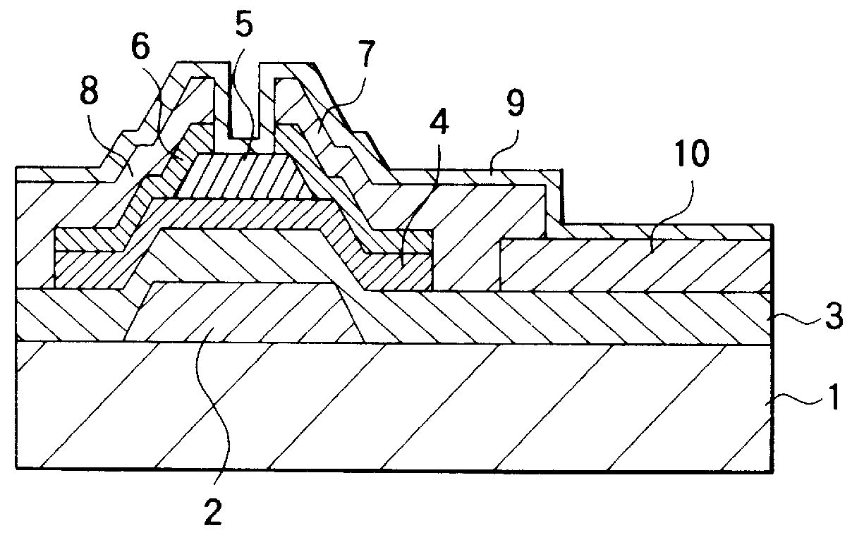
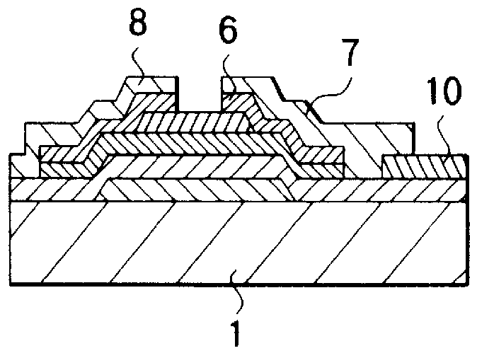
On the main surface of this active element substrate 26 which confronts the counter substrate 27 of the transparent insulating substrate 1 made of glass, a TFT 30 which is composed of a gate electrode 2, a gate insulating film 3, a semiconductor film 4, a etching stopper film on channel 5, an n type semiconductor film 6, a source electrode 7, a drain electrode 8, and an insulating protective film 9 as shown in FIG. 1 and a pixel electrode 10 are formed. Further, an aligning film 31 made of a cold curing type polyimide resin, for example, is provided on the TFT 30 and the pixel electrode 10. A polarizer 3...


PUM

PropertyMeasurementUnit
thicknessaaaaaaaaaa
thicknessaaaaaaaaaa
diameteraaaaaaaaaa

Abstract

A method for forming a multilayer film by introducing a material gas into a reduced-pressure reaction chamber provided with a pair of parallel planer electrodes and supplying a high-frequency electric power to the electrodes thereby generating a plasma state therein and depositing a film on a substrate disposed on one of the electrodes, comprising the steps of (a) introducing a first material gas into the reaction chamber and supplying the high-frequency electric power to the electrodes thereby generating the plasma state and depositing a first film on the substrate, (b) introducing stepwise a preparatory gas and adjusting stepwise a distance between the electrodes, a pressure inside the chamber and a RF power supplied to the electrodes while continuously retaining the plasma state subsequently to step (a), and (c) introducing a second material gas into the reaction chamber while continuously retaining the plasma state thereby and depositing a second film on the first film. According to the method the surface between the films is desirably formed, and this cause a promotion of characteristics when applied to produce a multilayer films constitutes semiconductor device, a TFT and a solar cell for example.

Description

BACKGROUND OF THE INVENTION1. Field of the InventionThis invention relates to a method for the formation of a multilayer film and more particularly to a method for the formation of a multilayer film constituting itself such a semiconductor device as a thin-film transistor.2. Description of the Related ArtMethods for forming a multilayer film on a substrate by plasma discharge have been known for long. One of the methods utilizes parallel planar electrodes to generate plasma. This method consists in forming a deposited film on a substrate or on a film already formed on a substrate by introducing a material gas into a reduced-pressure reaction chamber provided with parallel planar electrodes and supplying a high-frequency electric power between the electrodes thereby generating a plasma therein. To generate the plasma state, a microwave discharge and a electron cyclotron resonance have been known other than high frequency discharge. A multilayer film is formed by repeating this proced...

Claims


Application Information

Patent Timeline
Patent Type & Authority Patents(United States)
IPC IPC(8): C23C16/22C23C16/509C23C16/24C23C16/34C23C16/50H01L21/336H01L21/02H01L21/205H01L21/318
CPCC23C16/24H01L21/02274C23C16/50C23C16/5096H01L29/66757H01L29/66765H01L21/02686H01L21/02422H01L21/0245H01L21/02532H01L21/0262H01L21/0217H01L21/02211C23C16/345H01L21/3185H01L29/786
Inventor KASHIRO, TAKESHI
Owner JAPAN DISPLAY CENTRAL CO LTD
Why Eureka
Try Eureka