Method of fabricating an SOI wafer and SOI wafer fabricated thereby

a technology of soi wafer and soi layer, which is applied in the field of surface treatment of wafers, can solve the problems of increasing the variation of the thickness of the soi layer, the limitations of thesimox method, and the thickness and thickness uniformity of the resultant soi layer

Inactive Publication Date: 2000-10-31
SHIN-ETSU HANDOTAI CO LTD
View PDF4 Cites 112 Cited by
  • Summary
  • Abstract
  • Description
  • Claims
  • Application Information

AI Technical Summary

Problems solved by technology

However, the SIMOX method has many problems in relation to the reliability of a buried oxide layer, the crystallinity of the SOI layer, and necessity of heat treatment at a temperature of 1300.degree. C. or higher.
However, since the thin film is formed by means of mechanical machining, there are limits to the thickness and thickness uniformity of the resultant SOI layer

Method used


Image

  • Method of fabricating an SOI wafer and SOI wafer fabricated thereby
  • Method of fabricating an SOI wafer and SOI wafer fabricated thereby
  • Method of fabricating an SOI wafer and SOI wafer fabricated thereby

Examples


example

Twenty-eight mirror-polished silicon wafers having a diameter of 150 mm (conductive type: p type; resistivity: 10 .OMEGA..cm) were prepared. These wafers were processed through steps 1 to 6 of Method B shown in FIG. 1 to thereby obtain 14 SOI wafers which have an SOI layer having a thickness of 870 nm. The major process conditions used in the method were as follows:

a) Thickness of buried oxide layer: 400 nm;

b) Conditions of hydrogen implantation: H.sup.+ ions, implantation energy: 150 keV, implantation dose: 8.times.10.sup.16 / cm.sup.2 ;

c) Conditions of heat treatment for delamination: in a N.sub.2 gas atmosphere, at 500.degree. C. for 30 minutes; and

d) Conditions of heat treatment for bonding: in a N.sub.2 gas atmosphere, at 1100.degree. C. for 2 hours.

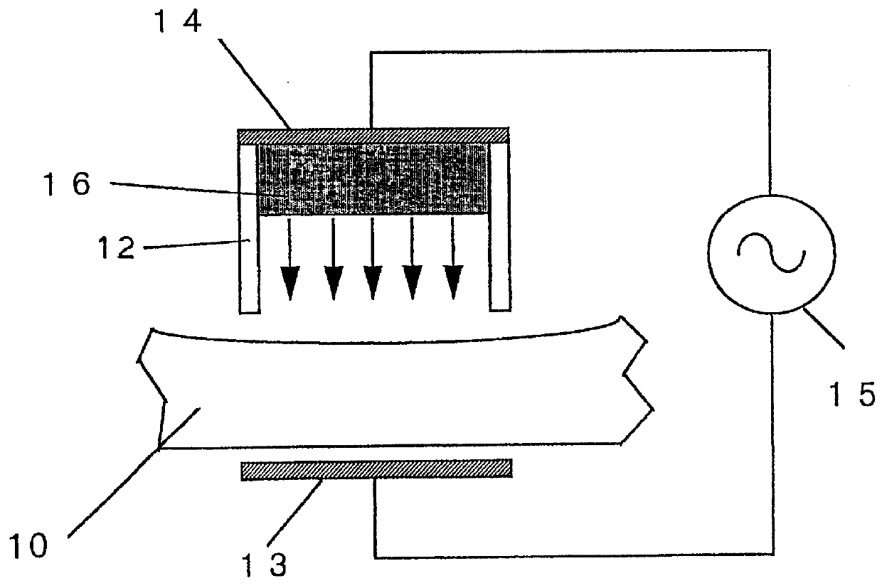
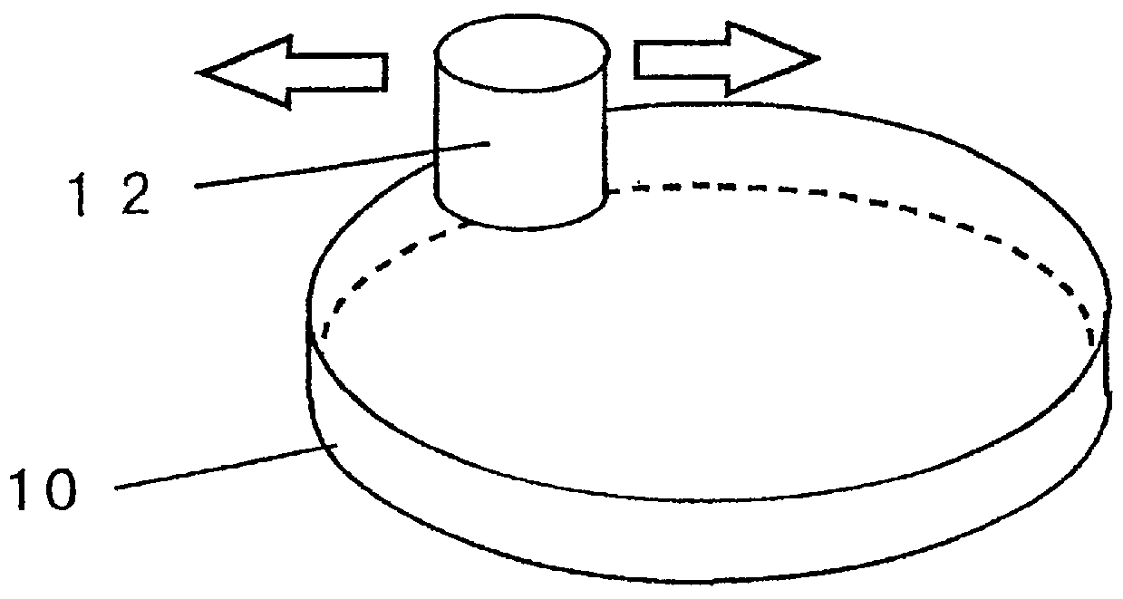
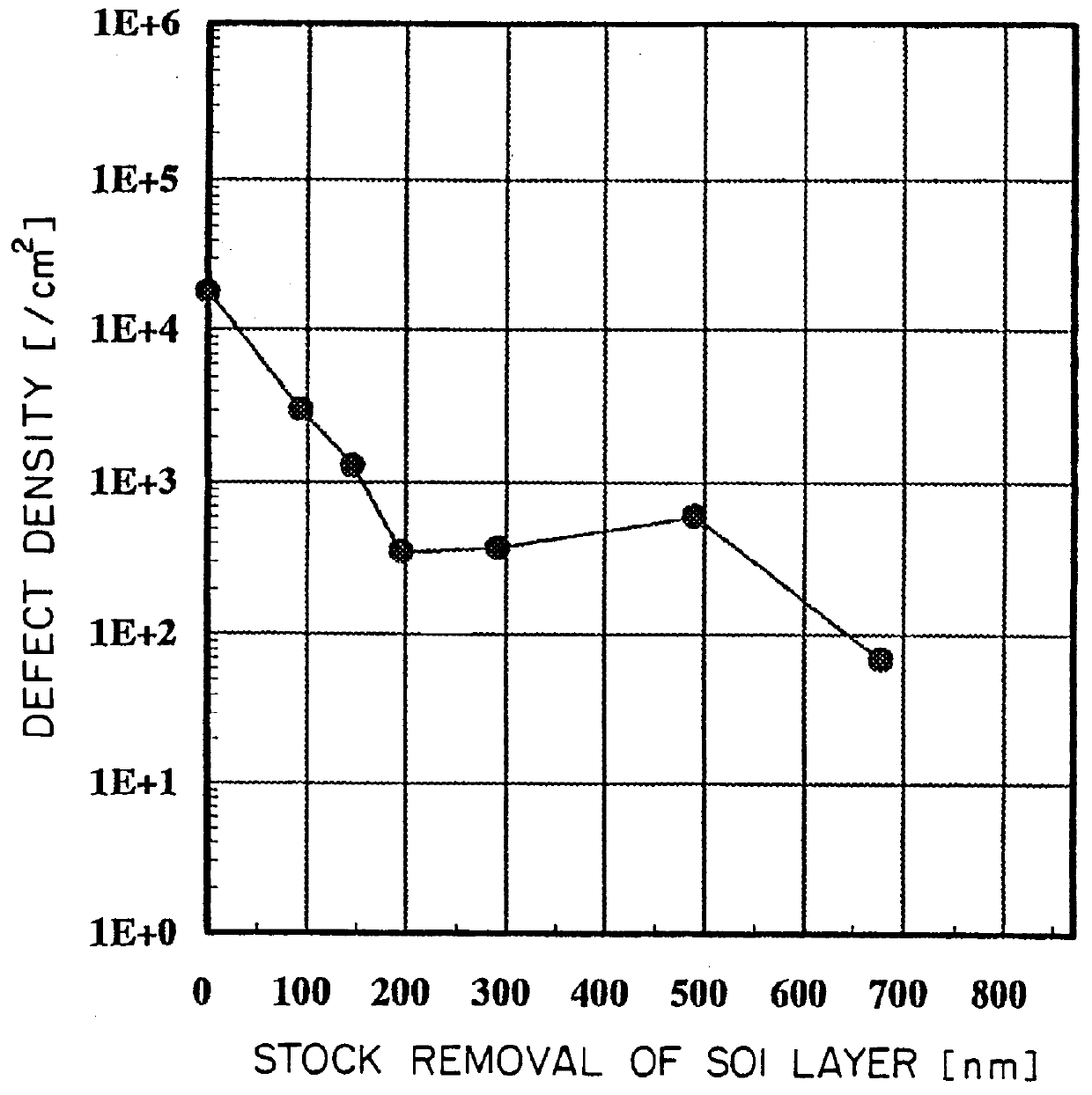
Of the thus-prepared SOI wafers, 12 SOI wafers were subjected to vapor-phase etching according to the PACE method two pieces at a time such that the SOI layer was etched to a depth of 90 nm, 140 nm, 190 nm, 290 nm, 490 nm, or 680 nm ...


PUM


Abstract

In a method of fabricating an SOI wafer, an oxide film is formed on the surface of at least one of two silicon wafers; hydrogen ions or rare gas ions are implanted into the upper surface of one of the two silicon wafers in order to form a fine bubble layer (enclosed layer) within the wafer; the ion-implanted silicon wafer is superposed on the other silicon wafer such that the ion-implanted surface comes into close contact with the surface of the other silicon wafer via the oxide film; heat treatment is performed in order to delaminate a portion of the ion-implanted wafer while the fine bubble layer is used as a delaminating plane, in order to form a thin film to thereby obtain an SOI wafer. In the method, a defect layer at the delaminated surface of the thus-obtained SOI wafer is removed to a depth of 200 nm or more through vapor-phase etching, and then mirror polishing is performed. Therefore, the obtained SOI wafer has an extremely low level of defects and a high thickness uniformity.

Description

1. Field of the InventionThe present invention relates to a surface treatment of a wafer having an SOI (silicon on insulator) structure which is fabricated in accordance with a method in which an ion-implanted wafer is bonded to another wafer and a portion of the ion-implanted wafer is delaminated to thereby obtain an SOI wafer (called a smart-cut method).2. Description of the Related ArtConventionally, two methods have gained wide notice as methods of fabricating wafers having an SOI structure. One method is a SIMOX (separation by implanted oxygen) method in which oxygen ions are implanted into a silicon monocrystal at a high concentration, and heat treatment is then performed at a high temperature in order to form an oxide layer. The other method is a bonding method in which two mirror-polished silicon wafers are bonded together without use of adhesive, and one of the wafers is subsequently made very thin.In the SIMOX method, the thickness of an SOI layer that becomes a device act...

Claims


Application Information

Patent Timeline
IPC IPC(8): H01L21/70H01L21/762H01L21/02H01L21/265H01L27/12
CPCH01L21/76254H01L21/76251H01L21/20
Inventor AGA, HIROJIMITANI, KIYOSHIINAZUKI, YUKIO
Owner SHIN-ETSU HANDOTAI CO LTD
Why Eureka
Try Eureka