Method for manufacturing compound semiconductor epitaxial wafer

a semiconductor and epitaxial wafer technology, applied in the direction of crystal growth process, polycrystalline material growth, chemically reactive gas growth process, etc., can solve the problems of degrading crystal quality and increasing slip dislocation

Inactive Publication Date: 2001-01-09
SHIN-ETSU HANDOTAI CO LTD
View PDF16 Cites 6 Cited by
  • Summary
  • Abstract
  • Description
  • Claims
  • Application Information

AI Technical Summary

Problems solved by technology

It was, however, made clear that an attempt to make sharp changes in vapor phase growth temperature corresponding to variation in the alloy composition, while making sharp changes also in the composition of a source gas containing group V elements in the periodic table (simply referred as group V source gas hereinafter) to be fed, to obtain the alloy composition gradient layer internally having sharp changes in the alloy composition, would often result in failure because of a large thermal capacity of a susceptor on which a substrate is placed, and a limited heat transmission rate from the susceptor to the substrate.
Instantaneous excessive heating and cooling to achieve drastic changes in the vapor phase growth temperature will result in slip dislocation more easily to degrade the crystal quality.

Method used


Image

  • Method for manufacturing compound semiconductor epitaxial wafer
  • Method for manufacturing compound semiconductor epitaxial wafer
  • Method for manufacturing compound semiconductor epitaxial wafer

Examples


Embodiment Construction

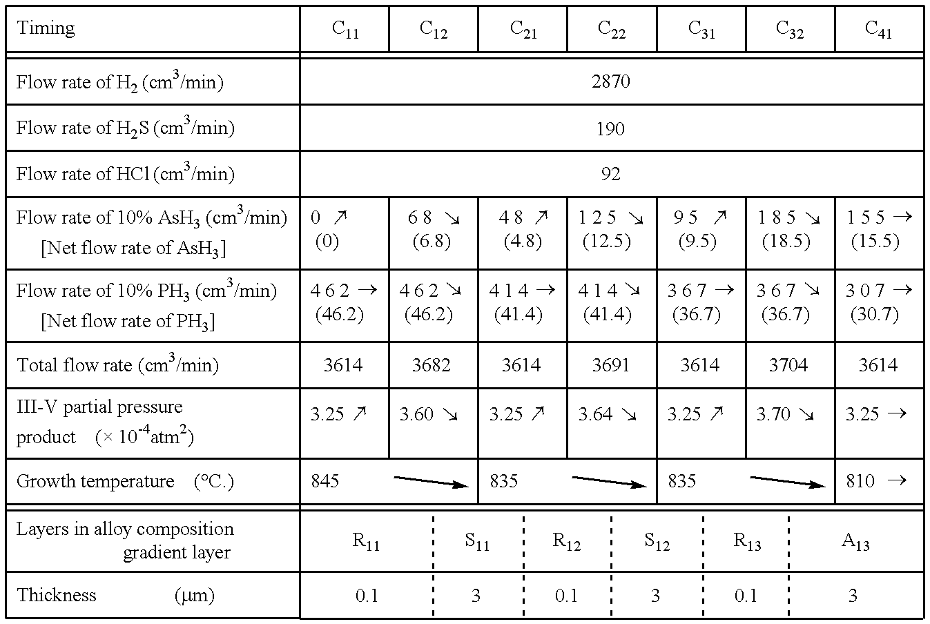
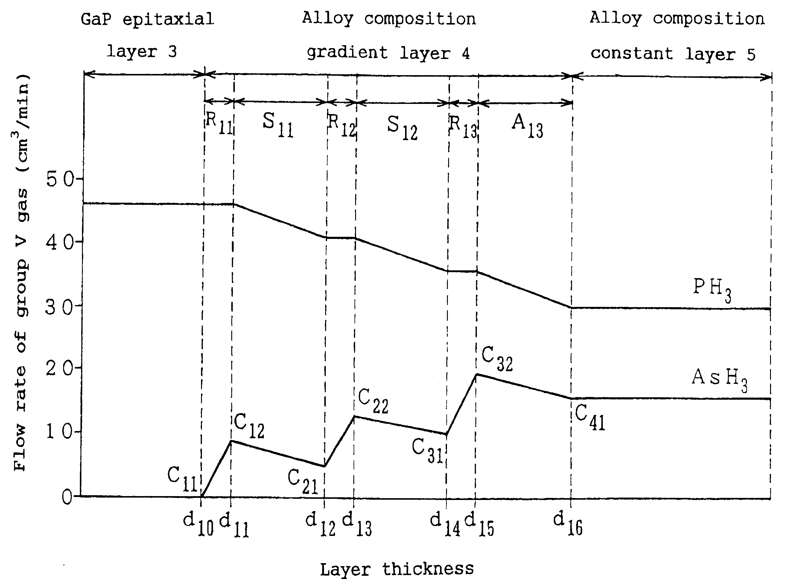
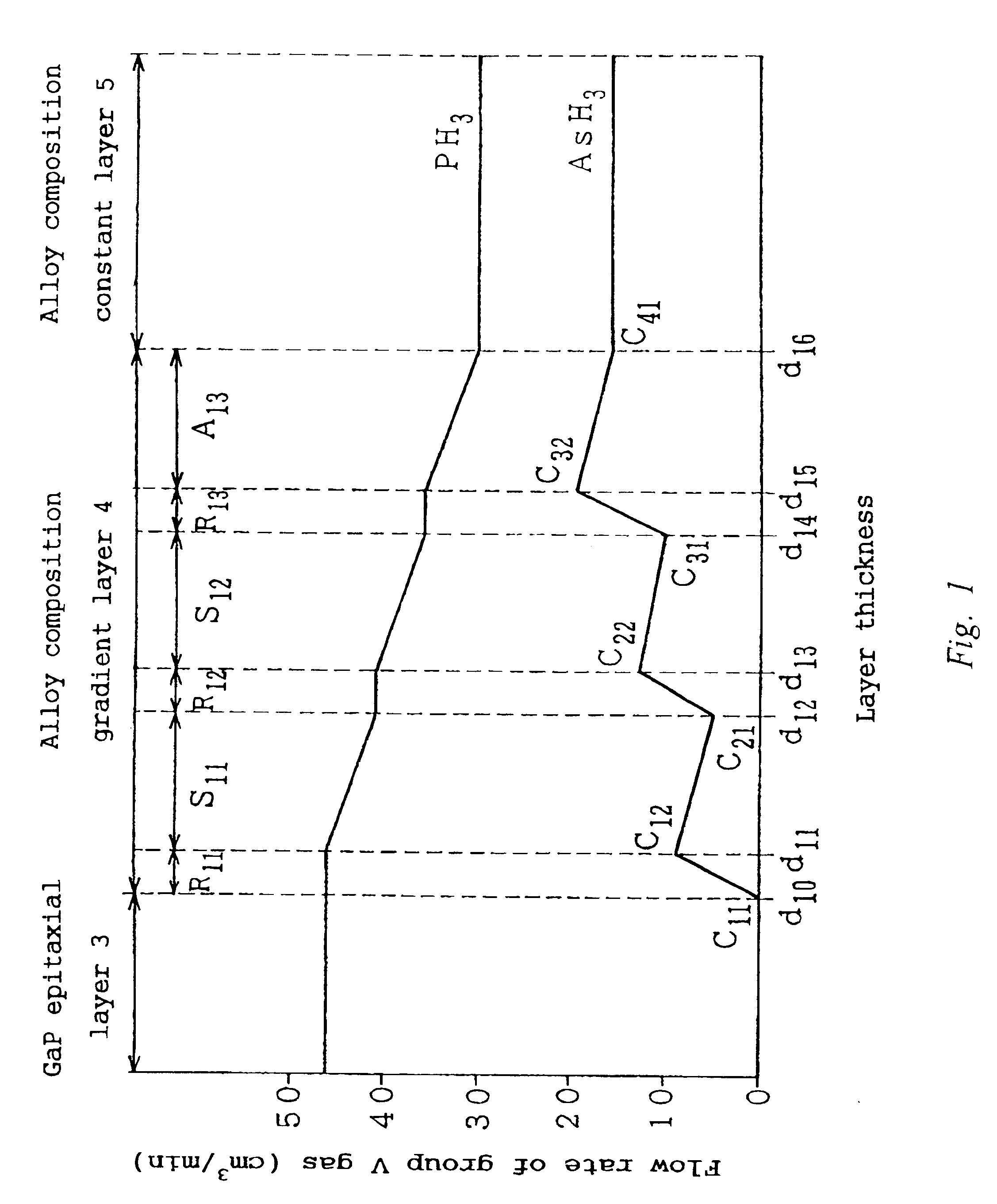
An epitaxial wafer 1 for an orange light emitting diode, including a gallium arsenide phosphide GaAs.sub.1-x P.sub.x alloy composition gradient layer 4 in which the alloy composition "1-x" of gallium arsenide GaAs ranges from 0 to 0.35 was manufactured according to the method described below.

An n-type gallium phosphide GaP single-crystalline ingot was sliced into a predetermined thickness, the slice was then subjected to chemical etching and mechanochemical polishing to obtain an approx. 300 .mu.m-thick mirror-finished gallium phosphide GaP wafer, which was used as a gallium phosphide GaP single-crystalline substrate 2.

The gases used in the vapor phase growth include hydrogen H.sub.2, hydrogen sulfide H.sub.2 S diluted to 50 ppm with hydrogen, arsine AsH.sub.3 diluted to 10% with hydrogen, phosphine PH.sub.3 diluted also to 10% with hydrogen, and high purity hydrogen chloride HCl.

In a normal pressure vapor phase growth furnace, in which the n-type gallium phosphide GaP single-crysta...


PUM

PropertyMeasurementUnit
thicknessaaaaaaaaaa
thicknessaaaaaaaaaa
off-angleaaaaaaaaaa

Abstract

A method for manufacturing compound semiconductor epitaxial wafer allowing sharp changes in alloy composition and growth of high-quality epitaxial layers. In a process for epitaxially growing a gallium arsenide phosphide GaAs1-xPx alloy composition gradient layer 4 on a compound semiconductor single-crystalline substrate made of gallium phosphide GaP or gallium arsenide GaAs, one group V gas as a source for the group V element not composing the single-crystalline substrate is varied in its supply volume in at least one cycle of sharp increase/moderate decrease, while the other group V gas as a source for the group V element composing the single-crystalline substrate is moderately decreased, thereby achieving at least one cycle of sharp increase/moderate decrease of a product of partial pressures of the group III and group V gases so that at least one set of an increasing zone and a decreasing zone of the alloy composition is formed within the gallium arsenide phosphide GaAs1-xPx alloy composition gradient layer 4.

Description

This disclosure relates to subject matter contained in Japanese patent application No. 152947 / 1997 (filed on May 27, 1997) and in No. 365057 / 1997 (filed on Dec. 19, 1997) Applicant hereby claims the priority of patent application 152947 / 1997 and patent application 365057 / 1997.1. Field of the InventionThis invention relates to a method for manufacturing compound semiconductor epitaxial wafer, more particularly to a method for manufacturing compound semiconductor epitaxial wafer having an alloy composition gradient layer.2. Description of the Prior ArtIn a field of manufacturing red light emitting diode or those emit orange or yellow lights, generally used is a compound semiconductor epitaxial wafer composing a single-crystalline substrate made of gallium phosphide GaP or gallium arsenide GaAs on which an alloy composition constant layer made of gallium arsenide phosphide GaAs.sub.1-a P.sub.a (where, "a" represents a real number satisfying 0.ltoreq.a.ltoreq.1) in which GaAs and GaP, t...

Claims


Application Information

Patent Timeline
Patent Type & Authority Patents(United States)
IPC IPC(8): C30B25/02H01L21/02H01L21/205C30B29/40H01L33/30
CPCC30B25/02C30B29/40H01L21/02392H01L21/02395H01L21/02461H01L21/02463H01L21/0251H01L21/02543
Inventor WATANABE, MASATAKAKAISE, TSUNEYUKISHINOHARA, MASAYUKI
Owner SHIN-ETSU HANDOTAI CO LTD
Why Eureka
Try Eureka