
Antenna device for generating inductively coupled plasma

Inactive Publication Date: 2001-09-11
JUSUNG ENG
View PDF10 Cites 91 Cited by
  • Summary
  • Abstract
  • Description
  • Claims
  • Application Information

AI Technical Summary

Problems solved by technology

In this regard, there are problems in the diode type plasma source like a difficulty in controlling high voltage and requirement of a high level of gas pressure, so that the diode type plasma source has not been suitable for processing such a fine pattern.
Even if an electron cyclotron resonance ("ECR") type plasma source is advantageous in obtaining a high density plasma under a low pressure, it is disadvantageous in achieving a uniform distribution of plasma.
Such a problem gets more severe as the size of plasma increases.
However, in case the size of plasma increases, the helicon wave type plasma source is not suitable for achieving a uniform density distribution of plasma.
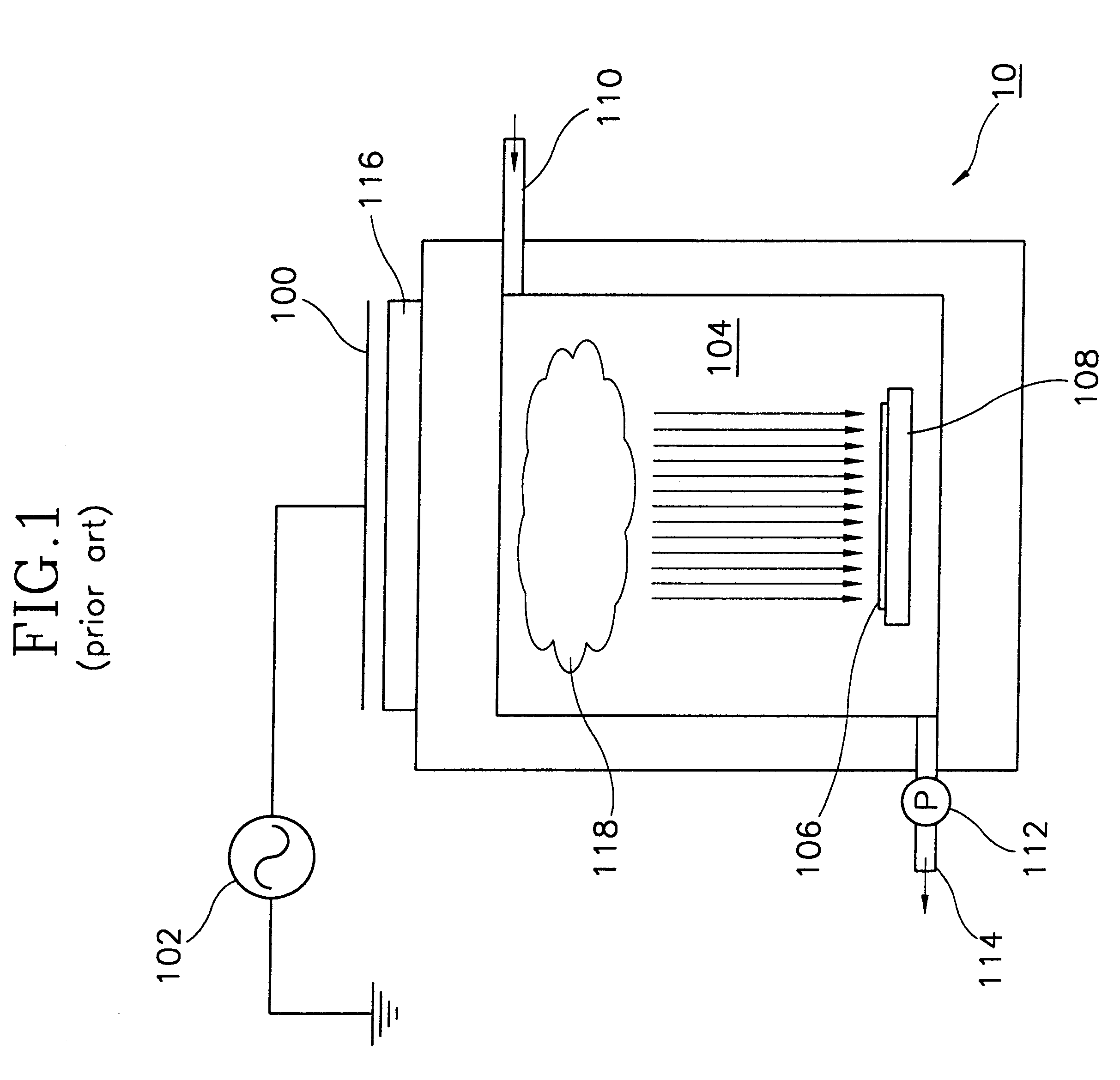
In this case, it is difficult to control distribution of inductive electric fields, and ions and electrons are lost at the internal wall of the chamber 104.
As a result, it is extremely difficult to achieve uniformity in the density distribution of the plasma 118.
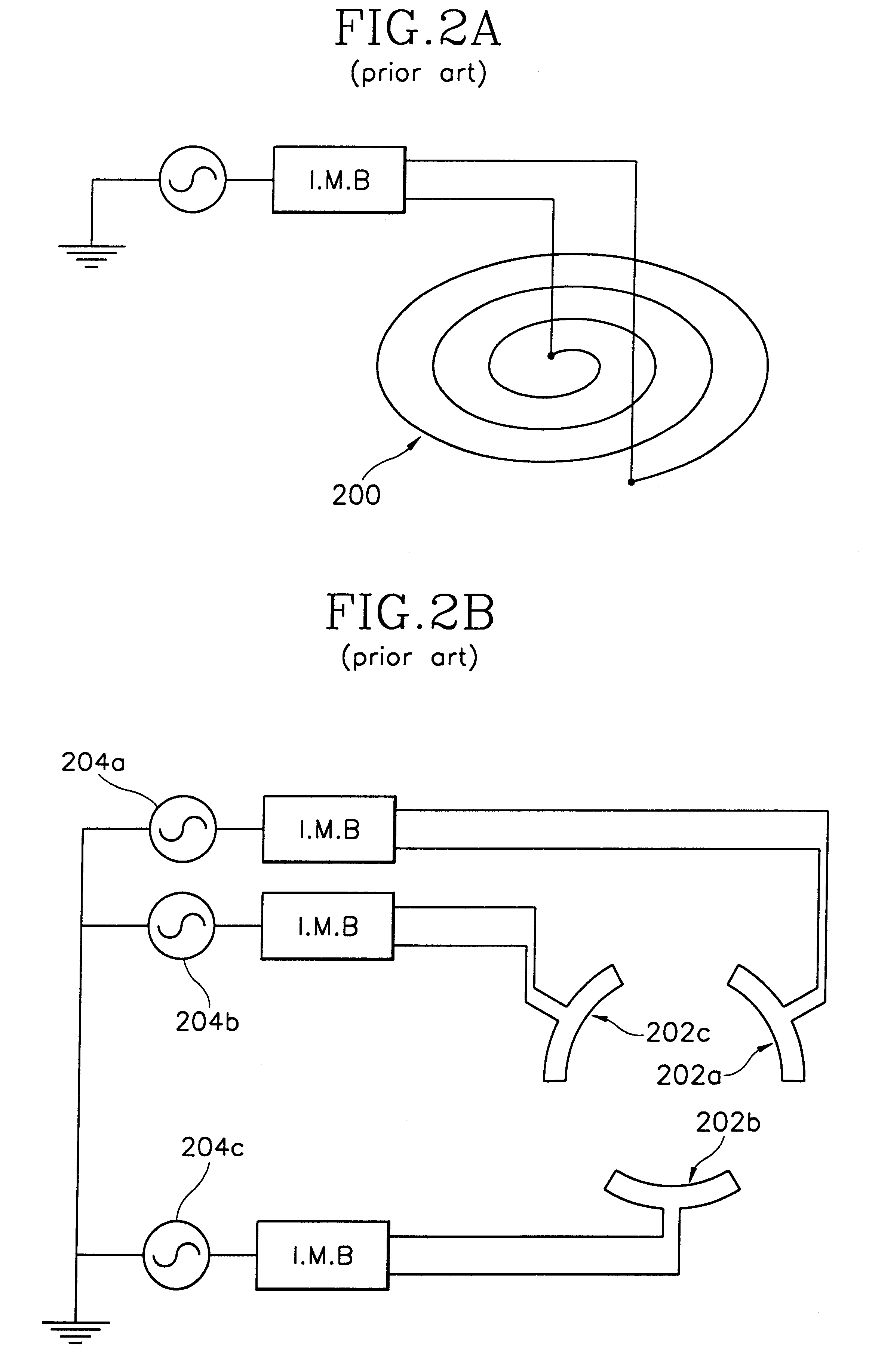
As a result, the electrical efficiency of the antenna 200 decreases and it is difficult to keep uniformity in the density distribution of plasma.
It is also difficult to ensure the uniformity in the density distribution of plasma, and it is more difficult to treat a large size of a specimen.
In addition, application of separately operated power results in increase in cost because an independent impedance matching circuit should be used for separate electrodes to achieve an impedance matching state for efficient uses of power.

Method used


Image

  • Antenna device for generating inductively coupled plasma
  • Antenna device for generating inductively coupled plasma
  • Antenna device for generating inductively coupled plasma

Examples


Embodiment Construction

Preferred embodiments of the present invention will be described in detail with reference to accompanying drawings.

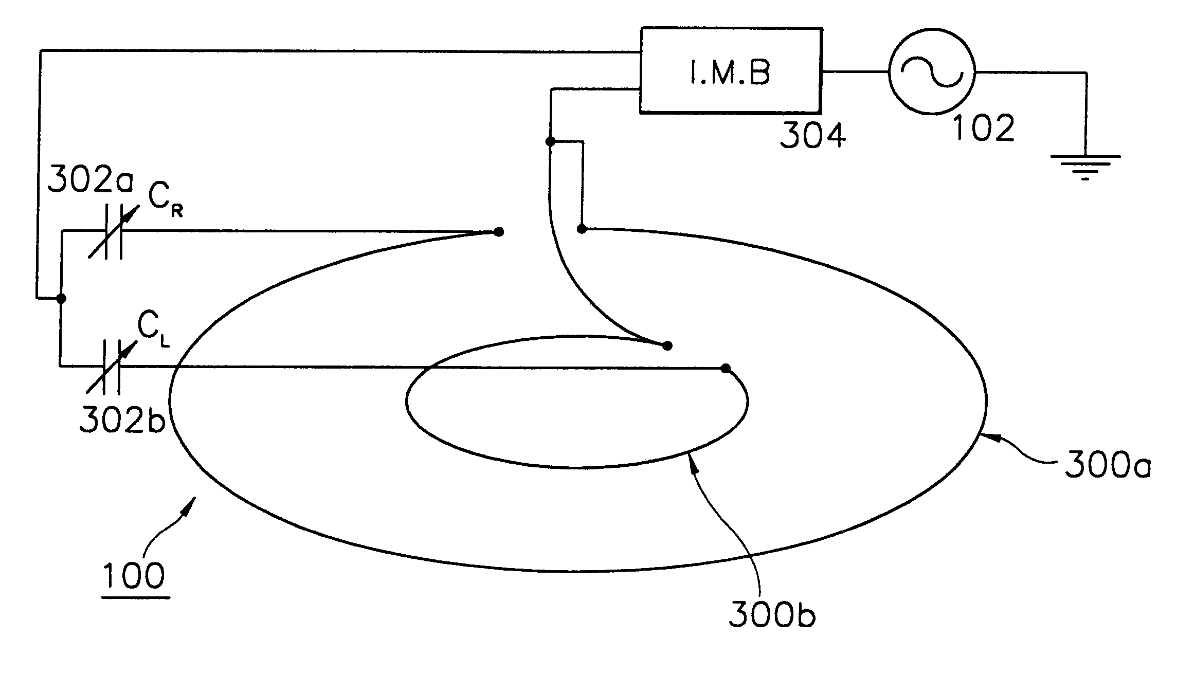
FIG. 3a is a conceptual view for illustrating an antenna device for generating inductively coupled plasma in accordance with an embodiment of the present invention, and FIG. 4a is an equivalent circuit diagram of an antenna device shown in FIG. 3a. As shown in FIGS. 3a and 4a, an antenna device 100 of the present invention includes a plurality of antenna units 400a and 400b connected in parallel with each other, which respectively include variable loads 302a and 302b and single or multi-wires of antennas 300a and 300b. In the antennas 300a and 300b, reference symbols R.sub.1, R.sub.2, and L.sub.1, L.sub.2 indicate resistance and equivalent inductance of respective antennas and capacitance of the antennas is absorbed and designated by reference symbols C.sub.R, C.sub.L respectively for resonance variable capacitance and variable load capacitance.

In addition, the antenna ...


PUM

PropertyMeasurementUnit
Frequencyaaaaaaaaaa
Electric impedanceaaaaaaaaaa

Abstract

The invention relates to an antenna device of a low impedance for generating a large quantity of inductively coupled plasma to process a large size of a specimen with adjustment for a uniform distribution in the density of plasma, comprising: a high frequency power source; a first antenna for receiving the high frequency power supplied from the high frequency power source; and a second antenna connected in parallel with the first antenna for receiving the high frequency power supplied from the high frequency power source, wherein a resonant state is kept between the first and second antennas.

Description

1. Field of the InventionThe present invention relates to an antenna device for generating plasma, and more particularly to an antenna device for generating inductively coupled plasma which can covers a large effective area to process a large specimen in a high, uniform density of plasma.2. Description of the Prior ArtIn order to produce a fine pattern on a substrate like a semiconductor wafer, flat panel display or the like in a technical field of fabricating a semiconductor device, plasma is generated to perform a variety of surface treatment process like dry etching process, chemical vapor deposition process, sputtering and the like. In order to reduce cost and improve throughput, the size of a semiconductor wafer and that of a substrate for a flat panel display has shown a tendency of getting larger, for instance, over 300 mm in recent years. Accordingly, a device for generating plasma to process such a large wafer or substrate also gets larger.Therefore, there have been plasma ...

Claims


Application Information

Patent Timeline
IPC IPC(8): H01J37/32H05H1/46C23C16/507H01Q1/27H01L21/205H01L21/302H01L21/3065
CPCH05H1/46H01J37/321H01Q1/27
Inventor LEE, YONG-KWANYOON, NAM-SIKKIM, SUNG-SIKLEE, PYUNG-WOOCHANG, HONG-YOUNG
Owner JUSUNG ENG
Learn More