However, a direct method of ODF measurement has not been developed.
However, use of these systems for texture determination, while feasible, is nonetheless time-consuming, lacks sufficient resolution, and is limited to relatively small
semiconductor wafers.
Furthermore, these current systems contain inherent limitations that make their conversion to a rapid, high precision measurement tool for large uncut wafers (e.g., 200
millimeter diameter, and recently introduced 300
millimeter diameter) problematic.
The speed of measurement, obtainable measurement resolution, and applicable wafer size remain as limitations of the state of the art in texture analysis of semiconductor wafers.
Using an area x-ray
detector on an x-ray
diffraction instrument increases the speed of texture analysis considerably, but area x-ray detectors are not currently used as efficiently as possible for texture analysis.
This is primarily due to the fact that they employ traditional texture analysis protocols that do not efficiently use all of the
diffraction information captured by the
area detector.
The
resultant measurement time is still quite long.
As a consequence, fewer samples are typically analyzed due to the excessive measurement times required.
Motion control systems have been built into x-ray diffraction systems for the mapping of texture over the surface of a large (e.g., 150 millimeter) wafer, but they too are not designed to make the most efficient use of diffraction information obtained from the
area detector.
Such
motion control systems also tend to be complex and very expensive.
Even if current x-ray diffraction systems utilizing area detectors were converted to map texture in larger wafers (by increasing the size of the
texture mapping stages), they would be extremely inefficient, complex, costly, and slow.
Efficient integration of a wafer
motion system (for mapping texture over the entire wafer surface) with an area x-ray detector has not been achieved with the currently available instruments.
The current texture analysis methodologies additionally are not suitable for new generations of materials (such as polycrystalline and epitaxial films, or superconductors) that have sharp textures.
The methods lack the required resolution, do not take
advantage of the sample and
crystal symmetry in order to expedite testing, and do not take
advantage of modern computing capabilities.
The current texture analysis methodologies do not make efficient use of all the diffraction data captured on an area x-ray detector.
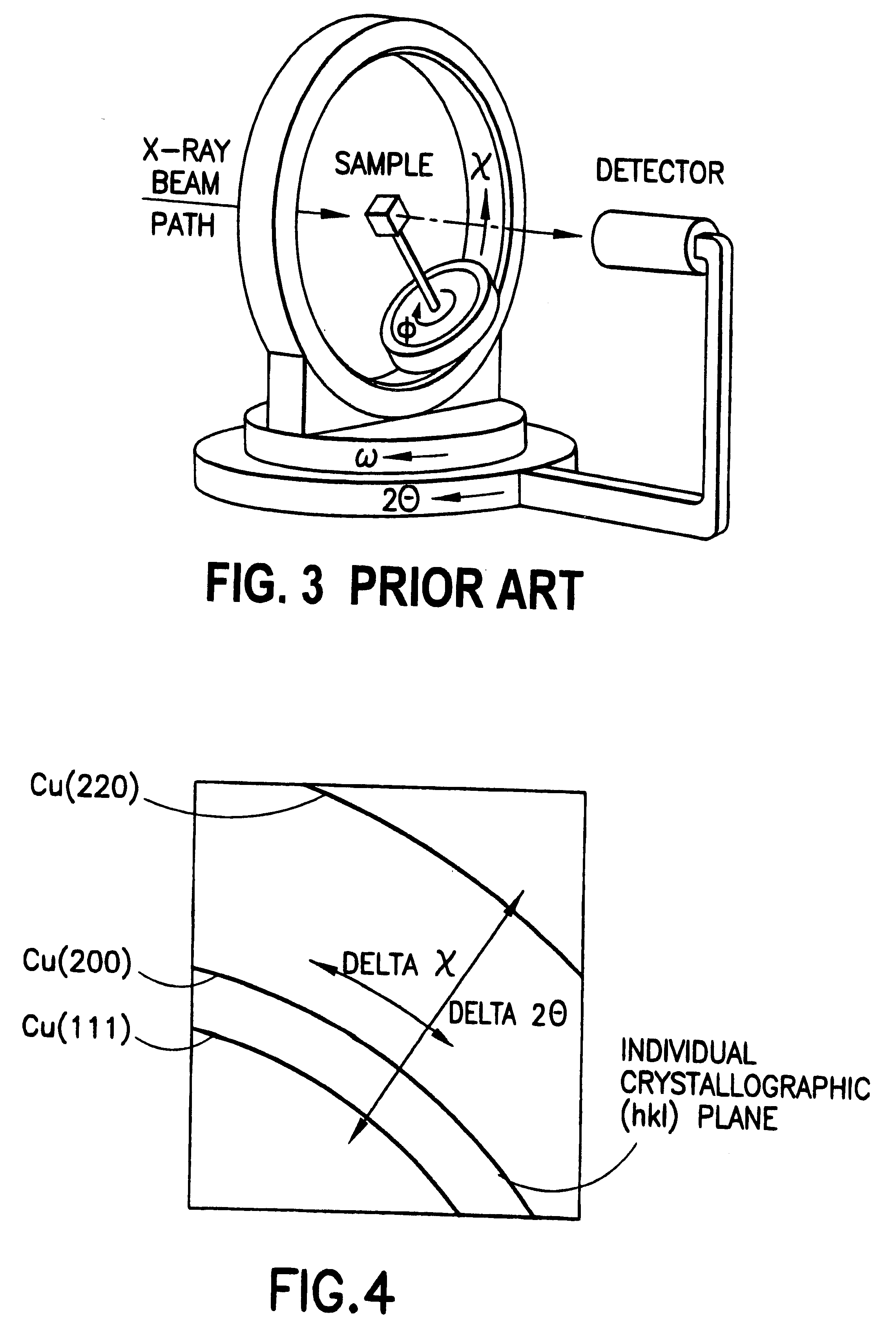
While texture analysis using current commercial x-ray systems is versatile, it is tedious, slow and requires a highly trained operator.
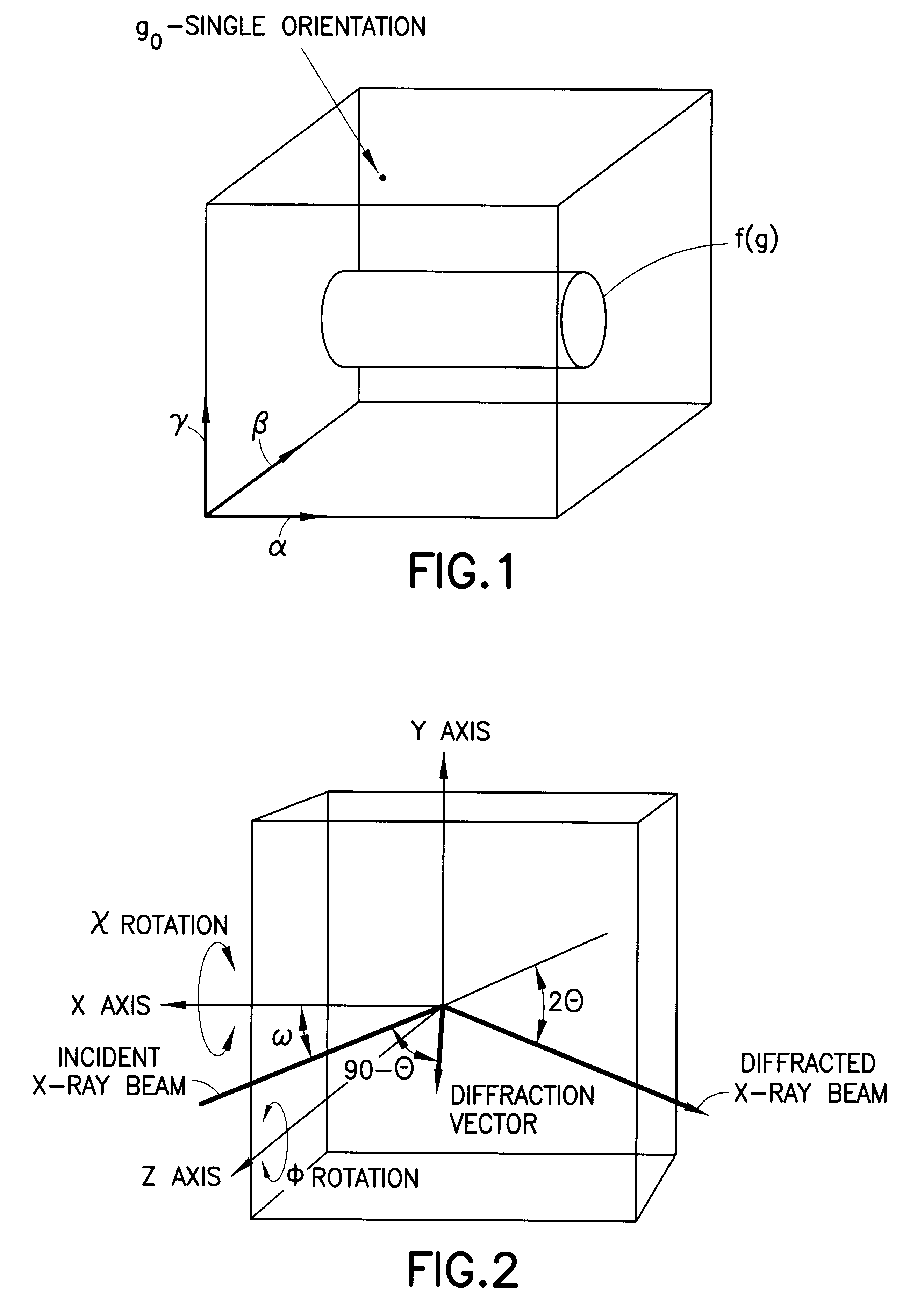
The central problem of quantitative texture analysis is the
reproduction of the ODF from experimental pole figures.
igures". Such a method required that a very thin isolated foil of material being tested be prepared and therefor is not practical as part of a commercial tes
One major drawback of the apparatus and measurement protocol described above is that it is relatively slow due to the large number of sequential scanning steps required with a
point detector.
Even so, measurements can require up to several hours.
This total
collection time does not account for the necessary corrections of the raw experimental data, and the computing time to calculate the ODF, which traditionally has also been a long procedure due to limitations on available computing power.
Thus, the excessive measurement times required to obtain pole figures independently using a
point detector represent a significant shortcoming of the prior art.
A further significant
disadvantage resulting from the long measurement times required by this approach is that the 5.degree. step scan can miss significant information in highly textured materials.
The primary reasons for the 5.degree. steps were a practical limitation in data collection times and limitations on computing power.
The computation time is several minutes since the algorithms do not make use of modem computing capabilities and are not optimized for speed.
Decreasing the step to 1.degree. would increase the computation time by a factor of 125, making it impractical for many of today's highly textured
engineering /
electronic materials.
Most traditional x-ray texture goniometers are not capable of handling
large size samples, or mapping over the surfaces of large samples.
However, such a
system would still exhibit several disadvantages.
First, the total wafer
motion control would be quite expensive in order to maintain wafer alignment, due to the use of the large Eulerian cradle which provides the sample .chi. rotation, in addition to supporting the other motion stages (x, y, z, and .phi.).
Making it large enough to
handle 200 mm wafers (8 inches), or 300 mm wafers (12 inches) would only exacerbate that cost.
A second major drawback is the large clearance distance required between the area detector and the contemplated combination of sample motion stages.
If the area detector is placed very close to the
measurement point the
angular range of 2.theta. and .chi. covered by the detector will be quite large, however the motion of the wafer will be severely restricted resulting in highly truncated pole figures.
This texture analysis protocol significantly increases the efficient use of a 2-D area x-ray detector for
texture mapping on semiconductor wafers, and thus significantly decreases
data acquisition time.

