Optical waveguide device and manufacturing method thereof

a technology of optical waveguides and manufacturing methods, applied in the direction of optical waveguide light guides, instruments, etc., can solve the problems of inability to manufacture thin film optical waveguides with a quality, inability to conduct diffusion or ion exchange of other elements, and inability to meet the requirements of material materials

Inactive Publication Date: 2001-10-23
EPIPHOTONICS CORP
View PDF5 Cites 60 Cited by
  • Summary
  • Abstract
  • Description
  • Claims
  • Application Information

AI Technical Summary

Problems solved by technology

This is chiefly because a thin film had to be grown epitaxially excepting for LiNbO.sub.3, for which the optical waveguide technique was established based on the single crystal growing technique and the Ti diffusion and proton exchange to a wafer thereof, so that a thin film optical waveguide could not be manufactured with a quality at a practical level by existent vapor phase growing, and because there was no available technique for manufacturing a waveguide lens even if the thin film optical waveguide per se could be manufactured.
However, in the method (1) of utilizing the difference of the thickness, the method (2) of coating the high refractive index layer and the method (3) of burying the high refractive index layer, coupling loss tends to be increased in principle, due to the presence of the step, by scattering at a lens boundary, lowering of overlap integral value and conversion of mode.
However, a method of conducting diffusion or ion exchange of other element is not available for the material other than LiNbO.sub.3, particularly, for Pb.sub.1-x La.sub.x (Zr.sub.y Ti.sub.1-y).sub.1-x/4 O.sub.3.
However, there is no available method for selectively applying etching without giving surface roughness which would lead to the s

Method used


Image

  • Optical waveguide device and manufacturing method thereof
  • Optical waveguide device and manufacturing method thereof
  • Optical waveguide device and manufacturing method thereof

Examples


example 1

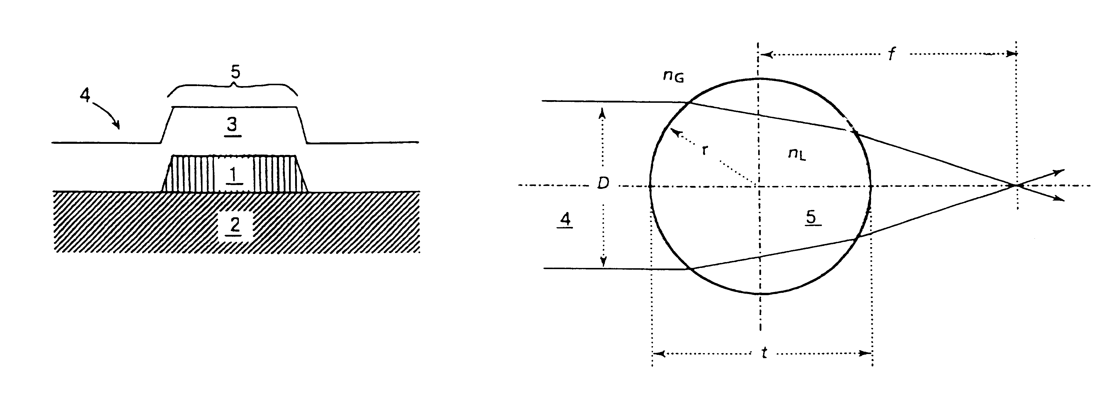
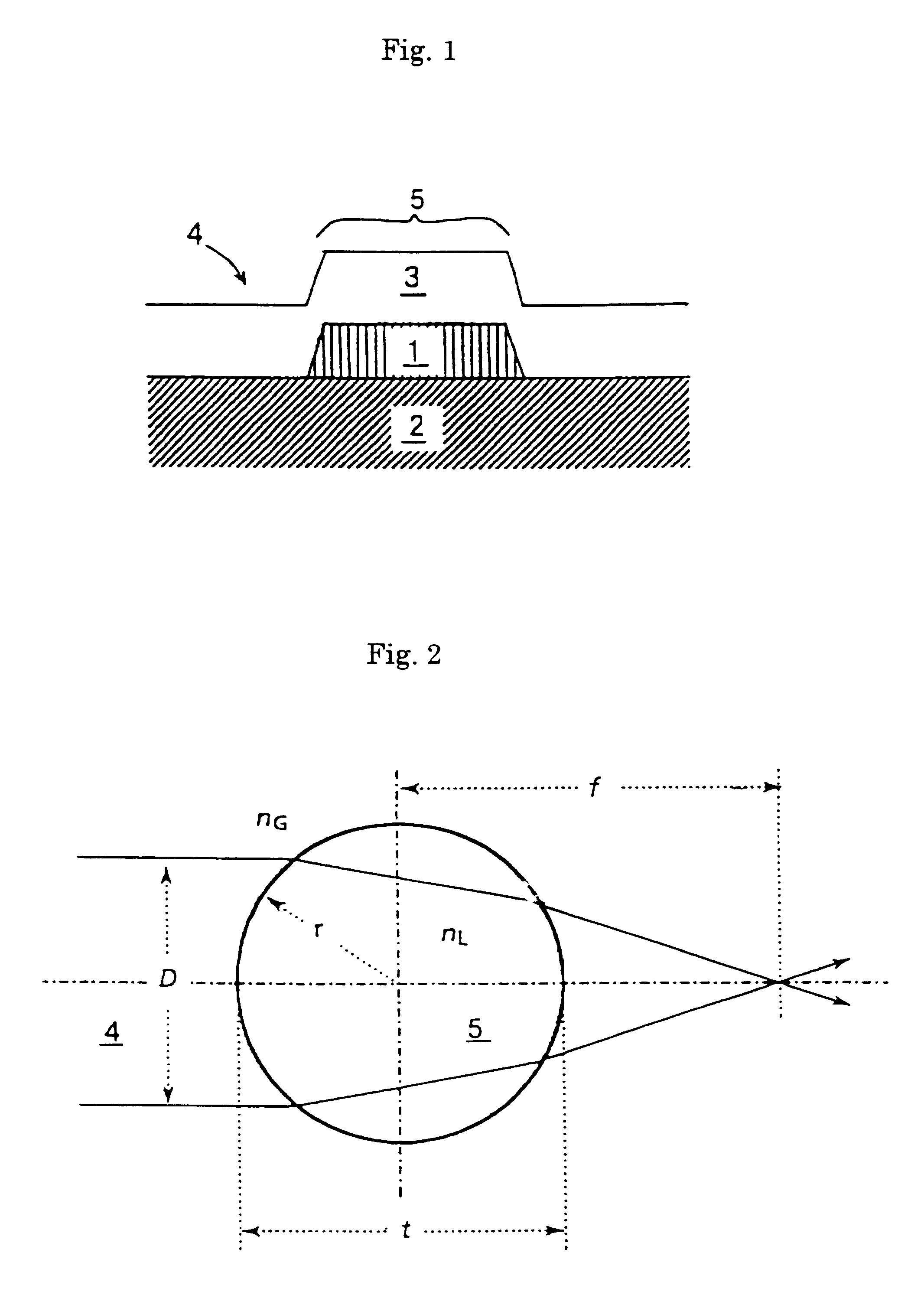
In this example, a circular lens of 800 .mu.m in diameter comprising, as shown in Table 1, a waveguide portion 4 of PLZT (9 / 65 / 35) thin film (film thickness=600 nm, n=2.49) / SrTiO.sub.3 substrate (n=2.40), and a lens portion 5 of PLZT (9 / 65 / 35) thin film (film thickness=600 nm, n=2.49) / PZT (30 / 70) thin film (film thickness=500 nm, n=2.61) / SrTiO.sub.3 substrate (n=2.40) and having a structure as shown in FIG. 1 and FIG. 2 was prepared and, further, a comb Al electrode was formed to the waveguide portion, to manufacture an optical switch based on the principle of an acousto-optic (AO) deflection device as shown in FIG. 10.

At first, anhydrous lead acetate Pb(CH.sub.3 COO).sub.2, zirconium isopropoxide Zr(O-i-C.sub.3 H.sub.7).sub.4 and titanium isopropoxide Ti(O-i-C.sub.3 H.sub.7).sub.4 were dissolved as starting materials in 2-methoxy ethanol and distilled and refluxed to finally obtain a precursor solution for PZT(30 / 70) at 0.6M of Pb concentration. Then, the precursor solution was spi...

example 2

In this example, a pupil type lens having 800 .mu.m of radius of curvature, comprising a waveguide portion 4 of PZT (52 / 48) thin film (film thickness =1000 nm, n=2.56) / SrTiO.sub.3 substrate (n=2.40), and a lens portion 5 of PZT (52 / 48) thin film (film thickness=1000 nm, n=2.56) / PZT (30 / 70) thin film (film thickness=800 nm, n=2.61) / SrTiO.sub.3 substrate (n=2.40) and having a structure as shown in FIG. 1 and FIG. 13 was manufactured.

At first, in the same manner as in Example 1, a precursor solution for PZT (30 / 70) was spin-coated on a cleaned, etched and dried SrTiO).sub.3 (100) single crystal substrate 2. Further, after elevating and keeping the temperature to 300.degree. C. in an O.sub.2 atmosphere, a power source for an electric furnace was tuned off to allow cooling. An epitaxial amorphous PZT(30 / 70) was obtained by repeating the procedures eight times. Then, after spin coating a positive resist and applying prebaking, UV-ray exposure was applied to a portion other than the pupil ...

example 3

In this example, a semi-pupil type lens having a radius of curvature of 800 .mu.m on one side, comprising a waveguide portion 4 of PLZT (9 / 65 / 35) thin film (film thickness=600 nm, n=2.49) / SrTiO.sub.3 substrate (n=2.40), and a lens portion 5 of PLZT (9 / 65 / 35) thin film (film thickness=600 nm, n=2.49) / PZT (30 / 70) thin film (film thickness=600 nm, n=2.61) / SrTiO.sub.3 substrate (n=2.40) and having a structure as shown in FIG. 1 and FIG. 14 was manufactured in the same manner as in Example 1.

At first, an amorphous PZT (30 / 70) thin film was obtained on an SrTiO.sub.3 (100) single crystal substrate 2 by use of a precursor solution for PZT (30 / 70). Then, electron beam exposure was applied to a semi-pupil type lens shape by use of an electron beam negative resist to form a semi-pupil type lens shape resist pattern. After etching the amorphous PZT (30 / 70) thin film with an aqueous HCl solution and peeling the resist, a first epitaxial PZT (30 / 70) thin film 1 of a semi-pupil type lens shape of...


PUM


Abstract

In an optical waveguide device, a laser beam is collected to an end face of a channel waveguide, and introduced into a PLZT thin film optical waveguide. The incident laser beam, when emitted from the channel waveguide, diverges in the PLZT waveguide, permeates a thin film lens and is collimated into 0.4 Mm size. When a high frequency voltage is not applied to a comb Al electrode, the laser beam is collected after penetrating through the second thin film and emitted from the end face through the channel waveguide to form an emission beam. When the high frequency voltage is applied to the comb Al electrode, a diffraction grating is formed by an acousto-optic effect, and the laser beam is deflected. The deflected laser beam, when penetrating through the second thin film lens, is collected and emitted from the end face through the channel waveguide in adjacent with the above-described channel waveguide to form a deflected emission beam.

Description

1. Field of the InventionThe present invention relates to an optical waveguide device having an optical waveguide of a ferroelectric thin film and a thin film lens for controlling a laser beam incident to the optical waveguide, and it has an application use in general optical integrated devices including, for example, optical deflection devices used for laser printers, digital copying machines and facsimile units optical switches and optical modulation devices used for optical communication and optical computers, and pick-up devices used for optical discs.2. Prior ArtFor disposing a deflection device, a switching or modulation device for a laser beam in an optical waveguide to constitute an optical integrated circuit device, it is important to form an electrode for deflection, switching or modulation to the optical waveguide, as well as use a waveguide lens for collimating a laser beam incident to the optical waveguide, and deflecting, switching or modulating and then collecting the...

Claims


Application Information

Patent Timeline
IPC IPC(8): G02F1/125G02F1/055G02F1/01G02B6/124G02B6/12G02B6/13
CPCG02B6/1245G02F1/0553G02F1/125G02B2006/12142G02B2006/12176G02B2006/12178
Inventor NASHIMOTO, KEIICHIHAGA, KOICHIWATANABE, MASAOMORIYAMA, HIROAKIMORIKAWA, TAKASHINAKAMURA, SHIGETOSHI
Owner EPIPHOTONICS CORP
Why Eureka
Try Eureka