

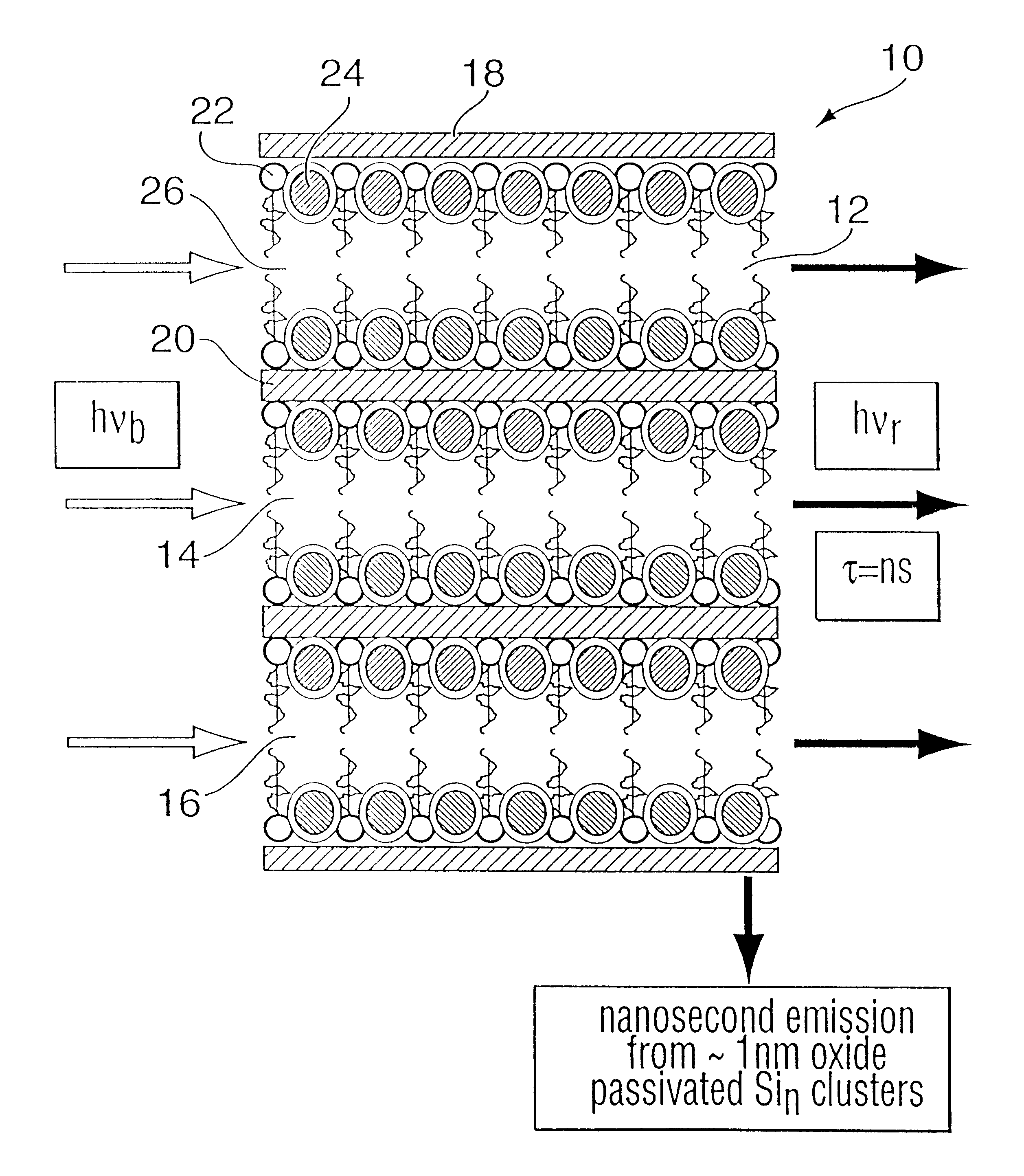
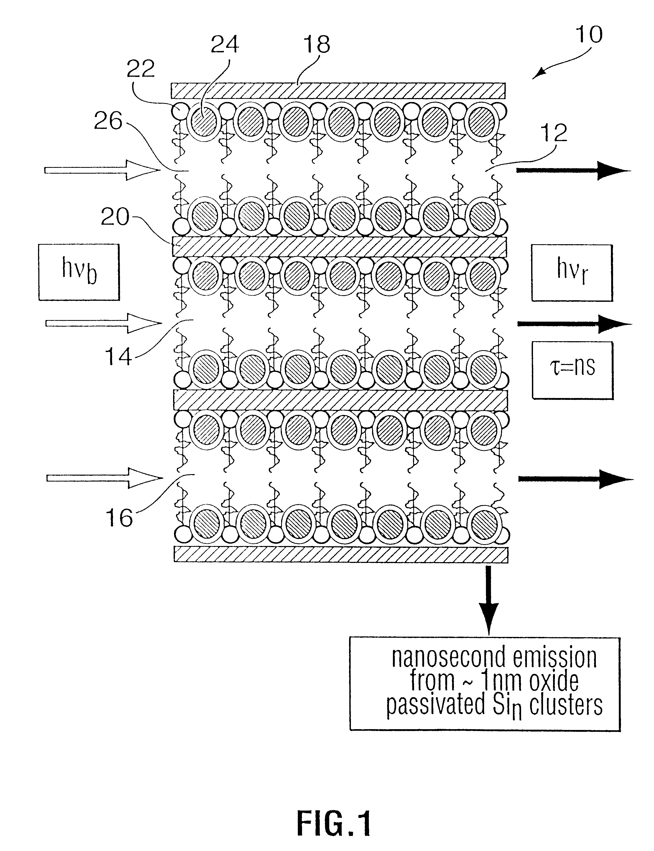
Fast luminescent silicon
a luminescent silicon and fast technology, applied in the field of optoelectronics, can solve the problems of inability to efficiently or fast emit light, degrade in ambient conditions in an hour, and silicon is an indirect band gap semiconductor
- Summary
- Abstract
- Description
- Claims
- Application Information
AI Technical Summary
Benefits of technology
Problems solved by technology
Method used
Image

Examples
example 2
5.89 g of a cetyltrimethylammonium chloride (CTACl) solution (29%) was mixed with 4.92 g of a HCl solution (36%) and 81.50 g of water. To this mixture was added 1.36 g of tetraethylorthosilicate (TEOS). The resultant mixture was stirred for 10 minutes at room temperature and then transferred to a high density polyethylene bottle. The mixture was set in a quiescent state at room temperature for about 11 days. The film grown at the water-HDPE (high density polyethylene) interface was easily peeled off from the HDPP and transferred from the solution to a substrate and dried in air. The disilane deposition was carried out in quartz vacuum sealed cells by dehydration of the film from 25.degree. C. to 100.degree. C. for 2 hours and 3 hours at 100.degree. C. Then 100 Torr of disilane was introduced and the reaction cell was heated at 140.degree. C. for 40 hours. The color of the resulting sample was yellow-orange in color. Photoluminescence (PL) has been observed for the films. The PL spec...
example 3
5.83 g of a cetyltrimethylammonium chloride (CTACl) solution (29%) was mixed with 4.94 g of a HCl solution (36%) and 81.54 g of water. To this mixture was added 1.37 g of tetraethylorthosilicate (TEOS). The resultant mixture was stirred for 10 minutes at room temperature and then transferred to a polypropylene bottle. The mixture was set in a quiescent state at room temperature. The free-standing film grown at the air-water interface was transferred to a substrate and dried in air. The disilane deposition was carried after dehydration of the film sample from 25.degree. C. to 100.degree. C. for 2 hours and 3 hours at 100.degree. C. Then 40 mg of disilane was introduced and the reaction cell was heated for 30 min from 25.degree. C. to 125.degree. C. and 15 hours at 125.degree. C. The resulting film sample was light yellow. Transmission electron microscopy images show the hexagonal mesostructure of the film after deposition.
example 4
5.83 g of a cetyltrimethylammonium chloride (CTACl) solution (29%) was mixed with 4.94 g of a HCl solution (36%) and 81.54 g of water. To this mixture was added 1.37 g of tetraethylorthosilicate (TEOS). The resultant mixture was stirred for 10 minutes at room temperature and then transferred to a HDPE bottle. The mixture was set in a quiescent state at ambient room temperature. The film grown at the water-HDPE interface was easily peeled off from the HDPE and was transferred from the solution to a substrate and dried in air. The disilane deposition was carried out in quartz vacuum sealed cells by dehydration of the film from 25.degree. C. to 100.degree. C. for 2 hours and 3 hours at 100.degree. C. Then 30 Torr of disilane was introduced and the reaction cell was heated at 140.degree. C. for 40 hours. The resulting film samples are yellow in color and yield orange PL. Temperature dependent PL, absorption-excitation-emission and polarized photoluminescence PL spectra are shown in FIG....
PUM
| Property | Measurement | Unit |
|---|---|---|
| diameter size | aaaaa | aaaaa |
| size | aaaaa | aaaaa |
| photoluminescence quantum efficiency | aaaaa | aaaaa |
Abstract
Description
Claims
Application Information