Semiconductor device with electric converter element

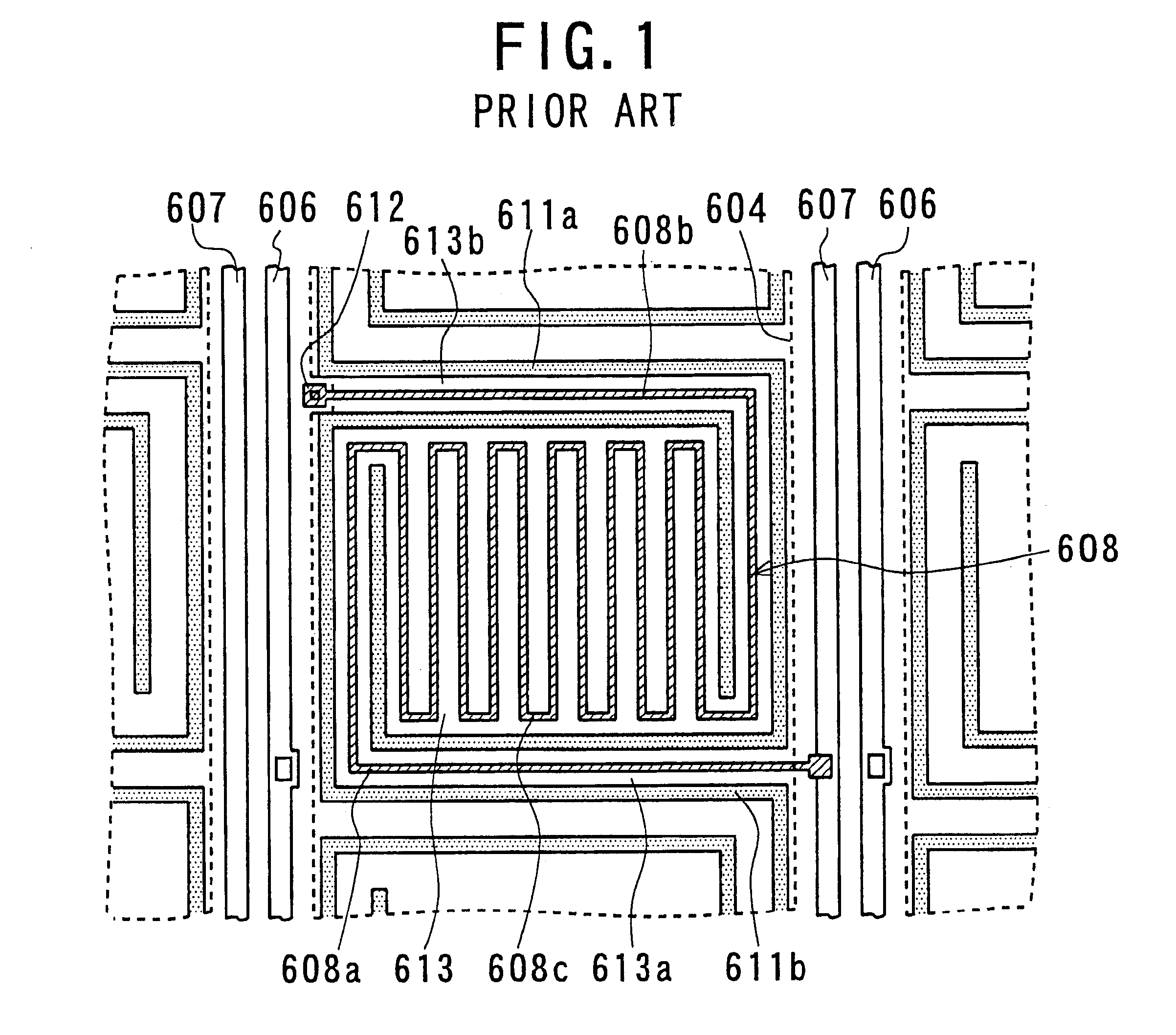
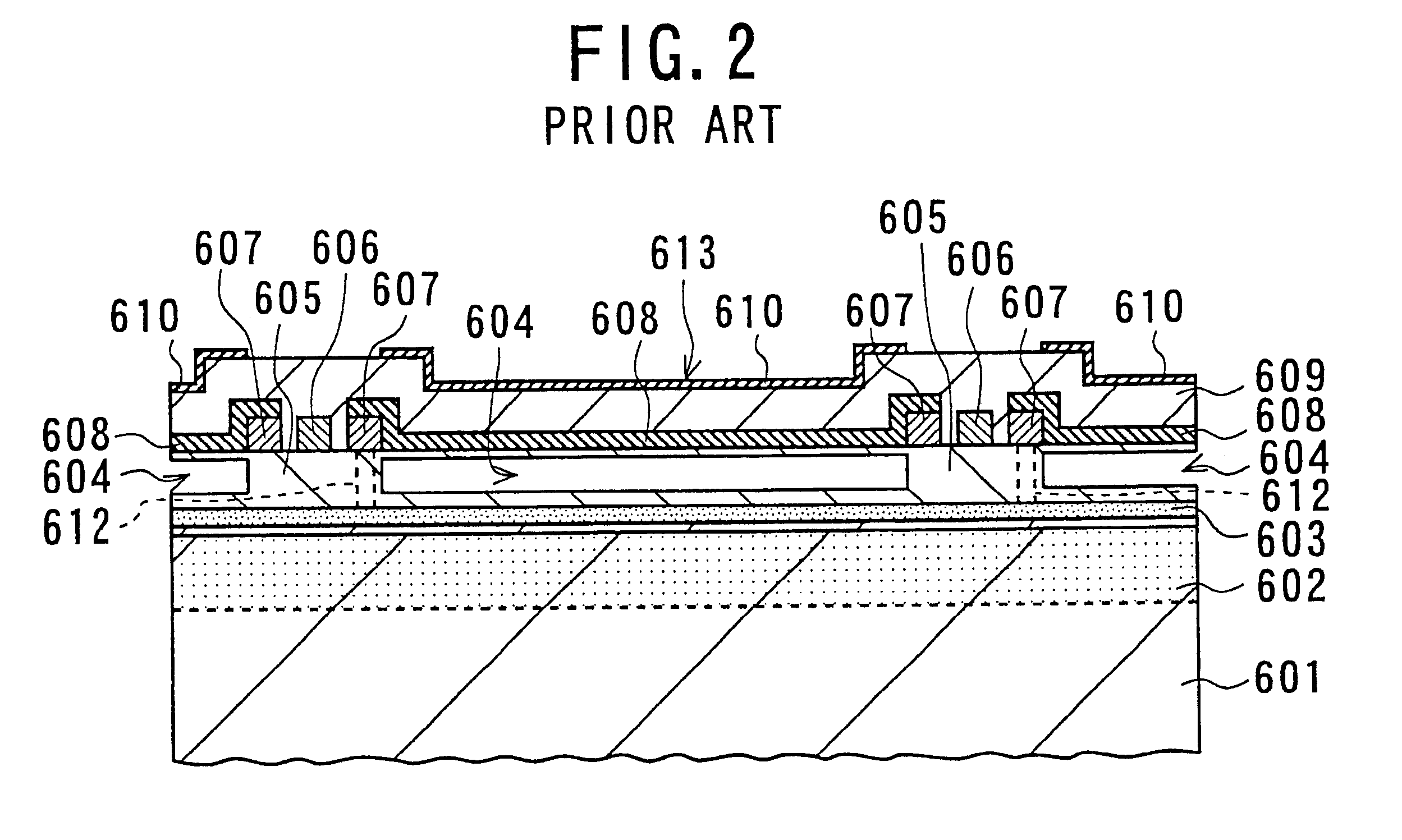
a technology of electric converter and semiconductor, which is applied in the direction of semiconductor/solid-state device details, optical radiation measurement, instruments, etc., can solve the problems of lowering the fabrication yield, unsatisfactory thermal shielding or blocking capability of the diaphragm 613, and unsatisfactory sensitivity of the bolometer 608

Inactive Publication Date: 2001-12-11
NEC CORP
View PDF21 Cites 36 Cited by
  • Summary
  • Abstract
  • Description
  • Claims
  • Application Information

AI Technical Summary

Problems solved by technology

A first problem is that the thermal shielding or blocking capability of the diaphragms 613 is unsatisfactory.
However, in this case, there is the same problem as above.
However, in this case, there arises another problem that the mechanical strength of the legs 613a and 613b is lowered The decrease of the mechanical strength of the legs 613a and 613b increases the danger that the diaphragm 613 is mechanically contacted with the underlying SiO.sub.2 layer 605 due to fluctuation or deviation of the process parameters in the fabrication process sequence of the conventional

Method used


Image

  • Semiconductor device with electric converter element
  • Semiconductor device with electric converter element
  • Semiconductor device with electric converter element

Examples


first embodiment

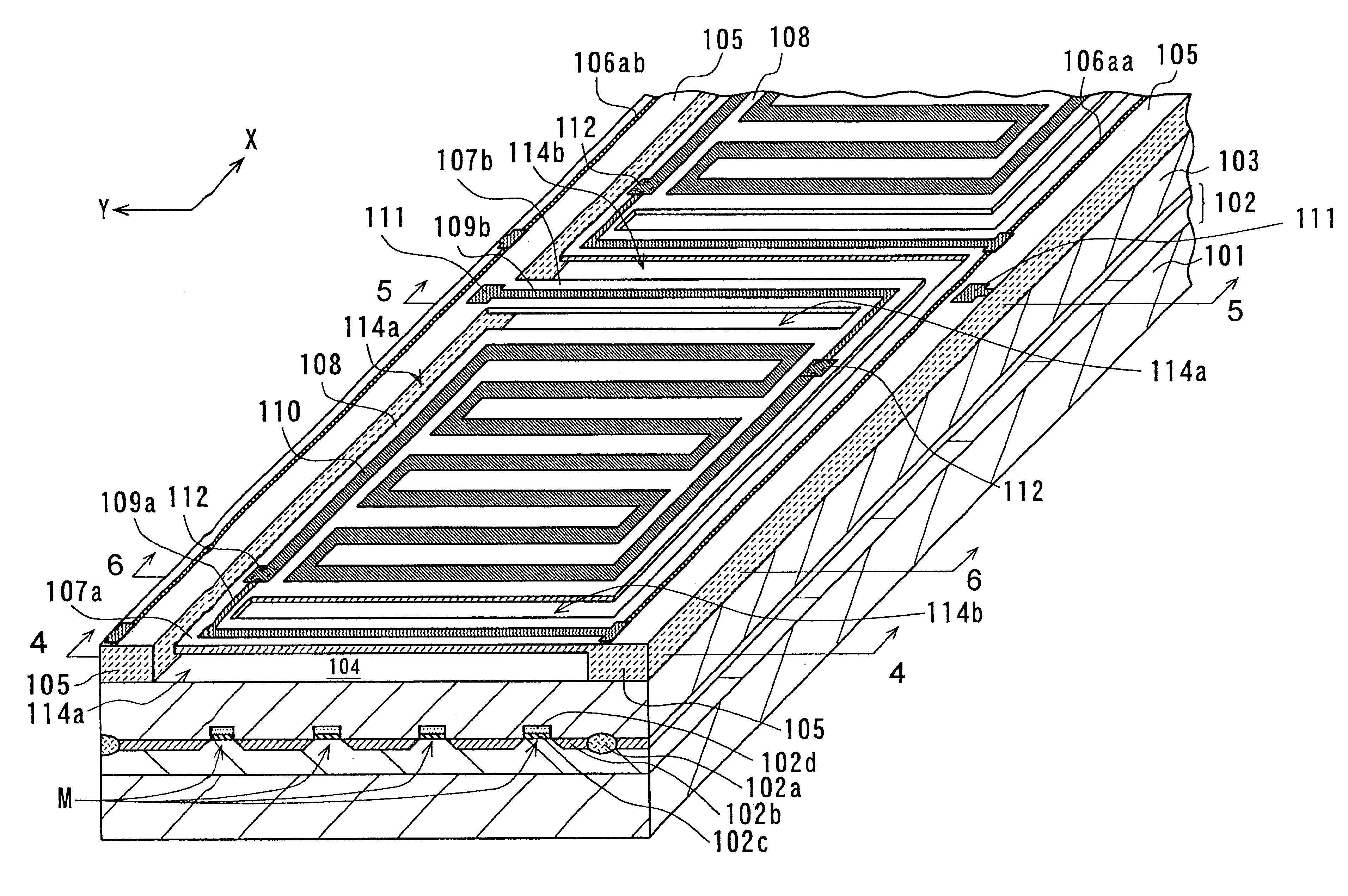
FIG. 3 schematically shows the configuration of a semiconductor device according to the present invention, which serves as an IR micro-sensor device.

As shown in FIG. 3, this semiconductor device includes a plurality of IR receiving sections or pixels arranged in a matrix array. Each of the IR receiving sections has a diaphragm 108 and thermoelectric converter (i.e., IR bolometer) 110.

An integrated circuit 102 is formed on a main surface of a single-crystal silicon (Si) substrate 101. The integrated circuit 102 includes a plurality of MOSFETs M formed in corresponding device regions, which are electrically isolated from one another by an isolation oxide 102a. Each of the MOSFETs M is formed by a pair of source / drain regions 102b, a gate oxide layer 102c, and a gate electrode 102d. The integrated circuit 102 is covered with an interlayer dielectric layer 103. Here, the layer 103 is made of SiO.sub.2.

A dielectric layer 105, which is made of SiO.sub.2, is formed on the interlayer dielec...

second embodiment

FIGS. 8, 9, and 10 show a semiconductor device serving as an IR micro-sensor device according to a second embodiment of the present invention.

This device according to the second embodiment has the same configuration as the first embodiment except that each of the bolometers 110 is made of the same material (i.e., titanium silicide) as the leg wiring lines 109a and 109b. Therefore, there is an additional advantage that the fabrication cost is lowered.

third embodiment

FIGS. 11 and 13 show a semiconductor device serving as an IR micro-sensor device according to a third embodiment of the present invention.

This device according to the third embodiment has the same configuration as the first embodiment except that the dielectric layer 201 is formed to cover central parts of the diaphragms 108. To cover the exposed parts of the diaphragms 108, a dielectric layer 202b is additionally formed.

Even if the tensile stress of the dielectric layer 201 is excessively strong, the warp of the diaphragm 108 may be adjusted by decreasing the area (i.e., size) and / or shape of the dielectric layer 201 it was found from the inventor's test that the after image problem was able to be prevented from occurring by adjusting the area or size of the dielectric layer 201 to be equal to 3 / 4 of the whole area of the diaphragm 108 or less. An example is shown in FIG. 14.


PUM


Abstract

A semiconductor device with an electric converter element on a diaphragm is provided, in which the diaphragm has an improved thermal shielding or blocking capability from a semiconductor substrate without lowering the mechanical strength of a leg of the diaphragm. The semiconductor device includes of a semiconductor substrate, a diaphragm mechanically connected to the substrate by a thermally-resistive leg, an electric converter element provided on the diaphragm, an electronic circuit formed on the substrate, and an electric path located on the leg for electrically connecting the electric converter element and the electronic circuit. The diaphragm is electrically insulated and thermally separated from the substrate. The electric converter element conducts a conversion between a physical quantity and an electric input/output signal. The electric path is made of a metal suicide to decrease its thermal conductivity without decreasing its electrical conductivity. The device is applicable to various sensors, generators, and actuators using heat.

Description

1. Field of the InventionThe present invention relates to a semiconductor device and more particularly, to a semiconductor devise with an electric converter element such as thermoelectric or electrothermal converter, which is applicable to various sensors, generators, and actuators using heat, such as an Infrared (IR)-ray sensor, flow sensor, gas sensor, pressure sensor, vacuum sensor, IR-ray generator, and manipulator.2. Description of the Prior ArtA semiconductor sensor device or semiconductor micro-sensor using heat is typically comprised of a semiconductor substrate, a heat-sensing or heat-input microstructure formed over the substrate and thermally shielded or separated therefrom, and an electronic circuit for processing an electric output signal from the microstructure. The microstructure usually has a thermoelectric converter element to produce the electric output signal according to the heat or temperature of the microstructure.An example of the conventional semiconductor se...

Claims


Application Information

Patent Timeline
IPC IPC(8): G01F1/684G01K17/20G01K17/00H01L29/66H01L21/3205H01L23/52H01L37/00
CPCG01F1/6845G01K17/20H01L29/66992H01L2924/0002H01L2924/00G01J5/046G01J5/10G01J5/20
Inventor TANAKA, AKIO
Owner NEC CORP
Why Eureka
Try Eureka