Electronic package with high density interconnect layer

a multi-layer interconnect and electronic package technology, applied in the direction of printed element electric connection formation, electrical apparatus construction details, association of printed circuit non-printed electric components, etc., can solve the problems of significant reliability concerns, and high stress on the interconnection between the organic chip carrier and the printed circuit board. , to achieve the effect of high density, high density and convenient subsequent deposition of conductive metal

Inactive Publication Date: 2002-04-16
ULTRATECH INT INC
View PDF21 Cites 89 Cited by
  • Summary
  • Abstract
  • Description
  • Claims
  • Application Information

AI Technical Summary

Benefits of technology

The present invention has the advantage of using a material in the surface redistribution layer that reliably retains its structural integrity during thermal cycling operations and, in particular, satisfies the stringent standards of Thermal Acceptance Testing (TAT), to be described infra.
The present invention has the advantage of having a high density interconnect layer for providing a direct electrical path from the multi-layered interconnect structure to an external electronic device.
The present invention has the advantage o...

Problems solved by technology

If the coefficient of thermal expansion (CTE) of the semiconductor chip, the organic chip carrier, and the printed circuit board are substantially different from one another, industry standard semiconductor chip array interconnections to the organic chip carrier may be subject to high stress during thermal cycling operation.
Similarly, the industry standard ball grid array (BGA) interconnections between the organic chip carrier and printed circuit board may also be subject to high stress during operation.
Significant reliability concerns may then become manifest by failure of the connections or even failure of the integrity of the semiconductor chip (chip cracking).
These reliability concerns significantly inhibit design flexibility.
These limitations ...

Method used


Image

  • Electronic package with high density interconnect layer
  • Electronic package with high density interconnect layer
  • Electronic package with high density interconnect layer

Examples


Embodiment Construction

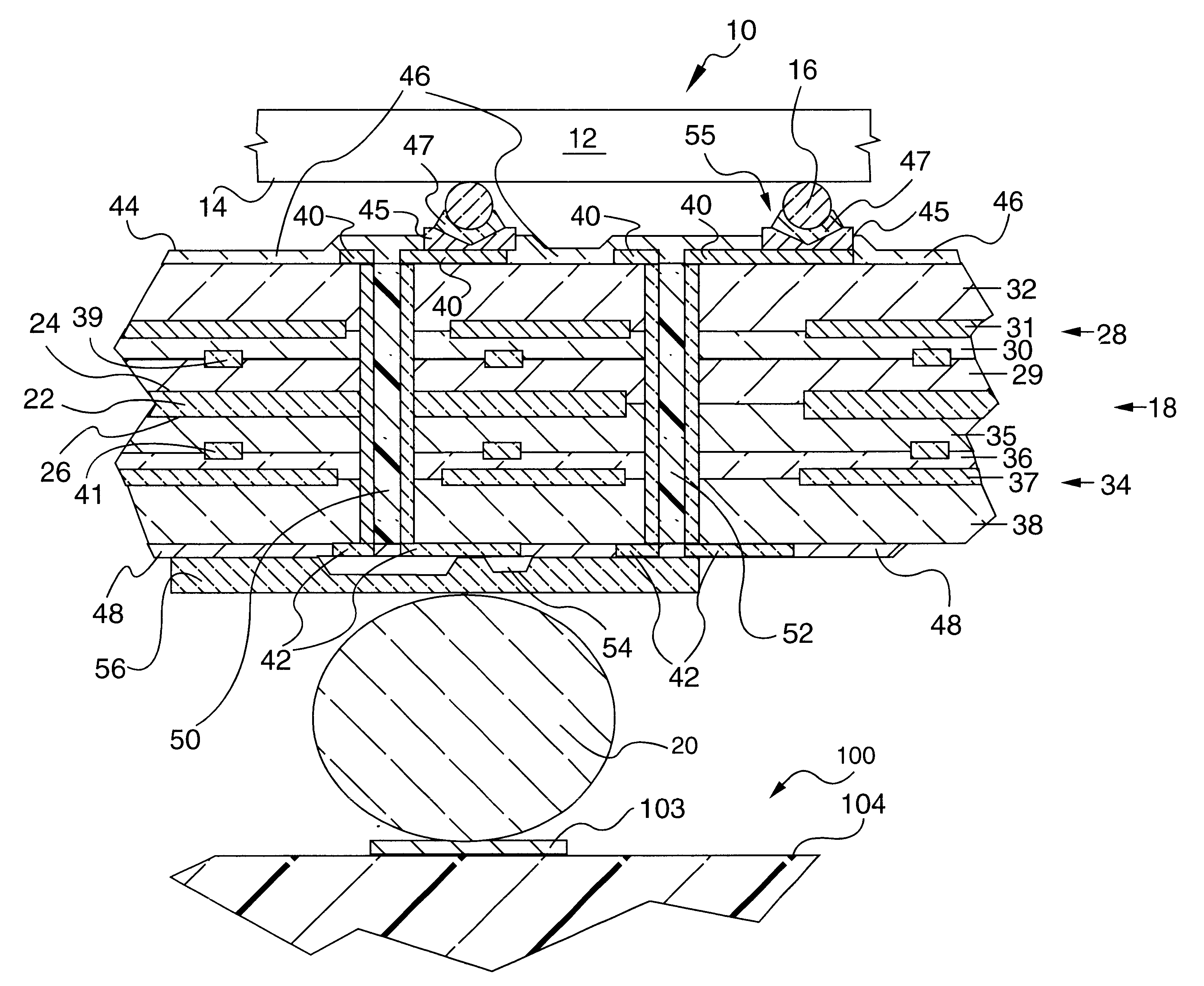
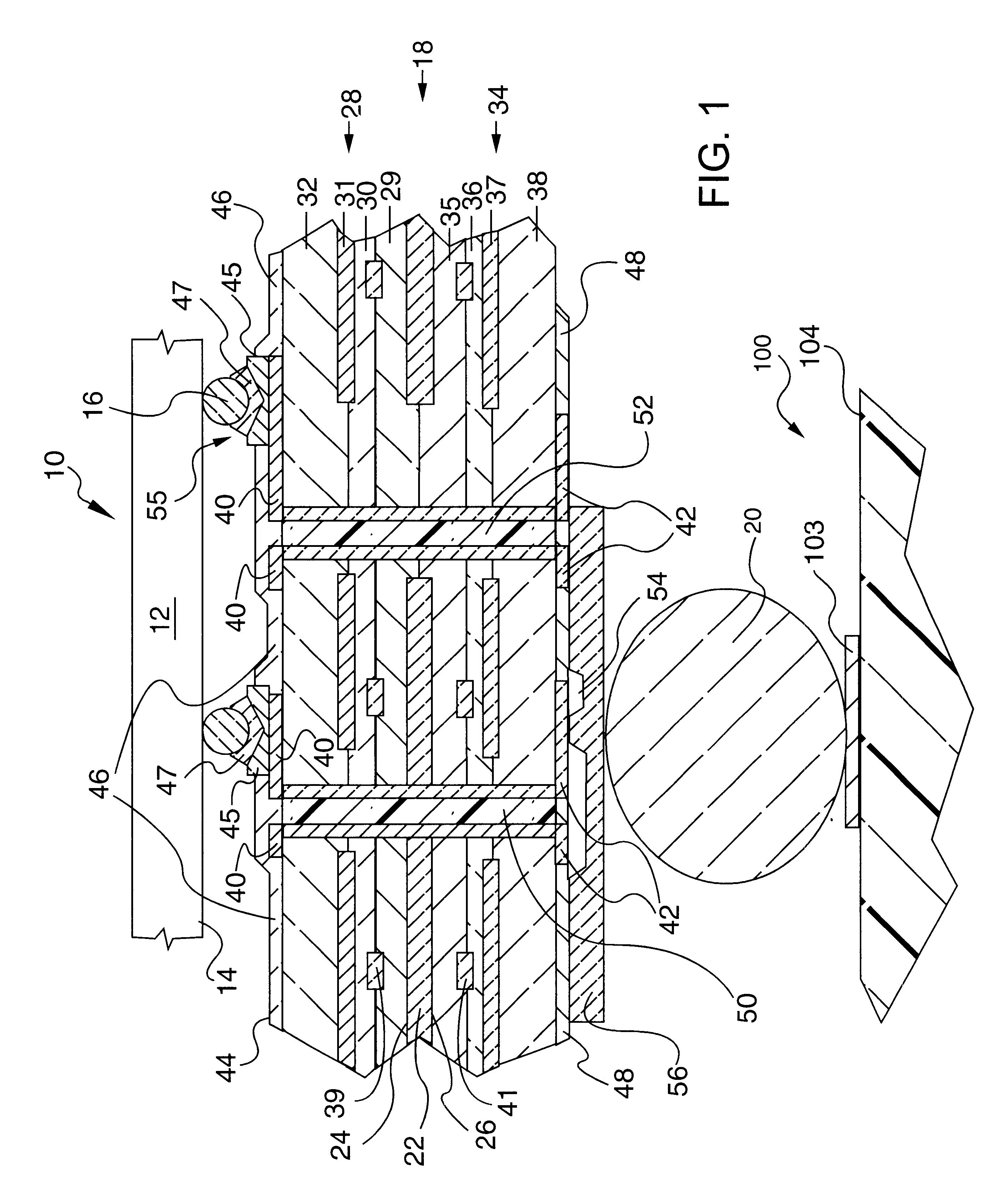
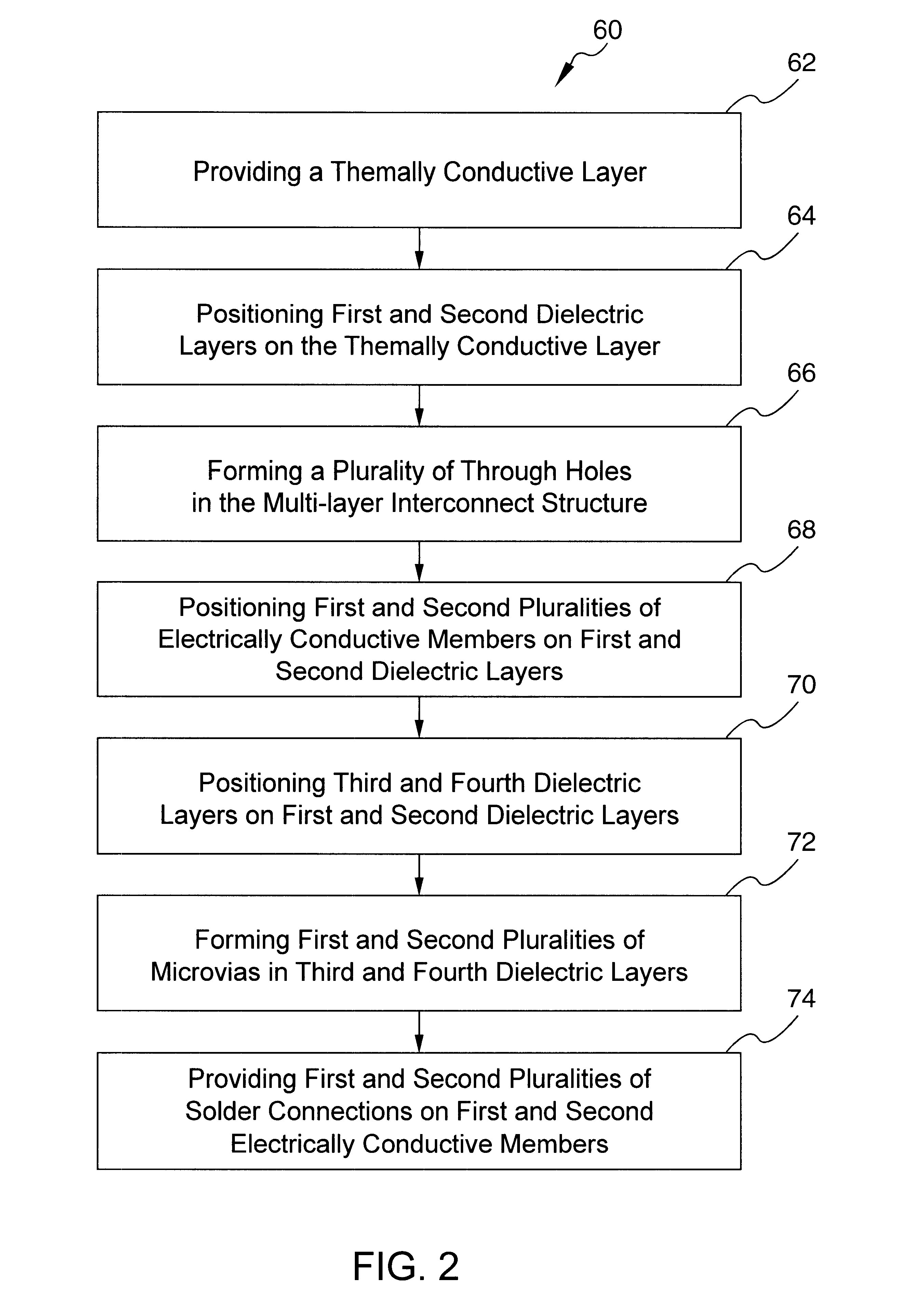
The present invention provides an electronic package which includes a multi-layered interconnect structure (e.g., a substrate comprising organic dielectric material, such as an organic chip carrier) and a semiconductor chip, the multi-layered interconnect structure being relatively compliant and having a coefficient of thermal expansion (CTE) of about 10 to about 12 ppm / .degree.C. which will not cause failure of interconnections between the semiconductor chip and a printed circuit board to which the package can be assembled. The multi-layered interconnect structure may be comprised of a single layer as an embodiment of the present invention. Failure of an interconnection, such as a solder interconnection, is defined as an increase of at least one ohm in electrical resistance of the interconnection as a consequence of being subjected to each test (i.e., test category) of Thermal Acceptance Testing (TAT), wherein the interconnection is actually tested under each TAT test or is alterna...


PUM

PropertyMeasurementUnit
Fractionaaaaaaaaaa
Fractionaaaaaaaaaa
Dielectric polarization enthalpyaaaaaaaaaa

Abstract

An electronic package, and method of making the electronic package, is provided. The package includes a semiconductor chip and an multi-layered interconnect structure having a high density interconnect layer such as an allylated surface layer. The semiconductor chip includes a plurality of contact members on one of its surfaces that are connected to the multi-layered interconnect structure by a plurality of solder connections. The multi-layered interconnect structure is adapted for electrically interconnecting the semiconductor chip to a circuitized substrate (eg., circuit board) with another plurality of solder connections and includes a thermally conductive layer being comprised of a material having a selected thickness and coefficient of thermal expansion to substantially prevent failure of the solder connections between said first plurality of electrically conductive members and the semiconductor chip. The electronic package further includes a dielectric material having an effective modulus to assure sufficient compliancy of the multi-layered interconnect structure during operation. The allylated surface layer has the property of being able to withstand thermal stresses that arise during thermal cycling operation of the electronic package.

Description

BACKGROUND OF THE INVENTION1. Technical FieldThe present invention relates, in general, to an electronic package for interconnecting a semiconductor chip to a printed circuit board, and in particular, to an organic multi-layered interconnect structure that includes a high density interconnect layer such as an allylated surface layer.2. Related ArtOrganic substrates, such as chip carriers, have been and continue to be developed for many applications. Organic substrates are expected to displace ceramic substrates in many chip carrier applications because of reduced cost and enhanced electrical performance. An organic substrate, such as an organic chip carrier for interconnecting a semiconductor chip to a printed circuit board in an electronic package, may have a surface redistribution layer for redistributing electrical signals from the chip into a larger area so that the chip can properly interface with the printed circuit board.As semiconductor chip input / output (I / O) counts increas...

Claims


Application Information

Patent Timeline
IPC IPC(8): H01L23/48H01L23/498H01L23/34H01L23/373H05K3/46H05K3/42H05K1/11H01L23/32H01L21/48
CPCH01L21/4853H01L23/49822H05K3/4608H05K3/4626H05K3/4632H05K3/4641H05K3/4688H01L23/3735Y10T29/49165H01L2224/16225H01L2924/01004H01L2924/01046H01L2924/01078H01L2924/12044H01L2924/15311H01L2924/3011H01L2924/3025H05K1/114H05K3/429H05K3/4602H05K3/4623H05K2201/0141H05K2201/0191H05K2201/068H05K2201/09509H05K2201/09536H05K2201/09554H05K2201/0959H05K2201/096H05K2201/10378H01L2924/01019H01L2924/01068H01L2924/01322Y10T29/49155H01L2924/00014H01L2224/0401
Inventor DOWNES, JR., FRANCIS J.FARQUHAR, DONALD S.FOSTER, ELIZABETHJAPP, ROBERT M.JONES, GERALD W.KRESGE, JOHN S.SEBESTA, ROBERT D.STONE, DAVID B.WILCOX, JAMES R.
Owner ULTRATECH INT INC
Why Eureka
Try Eureka