Method of improving vacuum quality in semiconductor processing chambers

a vacuum processing chamber and vacuum technology, applied in vacuum obtaining/maintenance, positive displacement liquid engines, lighting and heating apparatus, etc., can solve the problems of affecting the performance of thin films deposited by pvd and cvd processes, gaseous contaminants frequently, and significantly affecting the resistivity, grain structure, reflectivity, step coverage,

Inactive Publication Date: 2002-05-28
GLOBALFOUNDRIES INC
View PDF4 Cites 8 Cited by
  • Summary
  • Abstract
  • Description
  • Claims
  • Application Information

AI Technical Summary

Problems solved by technology

The presence of contaminants, such as water, nitrogen and carbon dioxide in the chamber can radically degrade the performance of thin films deposited by PVD and CVD processes.
Such gaseous contaminants frequently are the result of outgassing from the chamber walls of molecules left over from previous processing.
Irrespective of their particular origin, contaminants in the vacuum chamber can significantly impact the resistivity, grain structure, surface texture, reflectivity, step coverage, electromigration and circuit reliability associated with a deposited metal film.
Although these three pumping systems can achieve vacuums greater than 10.sup.-7 torr, they nevertheless exhibit certain limitations.
Diffusion pumps produce some degree of oil backstreaming that can lead to oil contamination of the vacuum chamber, while all three pumping systems have pumping speed limitations.
While the incorporation of plasma based test wafer conditioning speeds the conditioning of a vacuum chamber and improves the overall vacuum quality thereof, many semiconductor processing chambers do not utilize plasma processes and reactions, and thus cannot take advantage of the benefits of test wafer conditioning through plasma processing.
The main disadvantages associated with the conventional methods of conditioning vacuum chambers is the cost associated with the consumption of conventional conditioning wafers and the sheer length of the conditioning process due to the relatively slow pumping speeds of high vacuum pump systems.
This speed phenomena is particularly germane to the multitudes of non-plasma based processing chambers, which cannot take advantage of the speed enhancing characteristics of plasma based test wafer conditioning.
The technique inherently involves some contamination of the processing chamber with titanium and the species used to sputter the titanium into vapor phase.
This leads to difficult maintenance issues.
In addition, titanium gettering pumps have limited ability to provide very low pressures.

Method used


Image

  • Method of improving vacuum quality in semiconductor processing chambers

Examples


Embodiment Construction

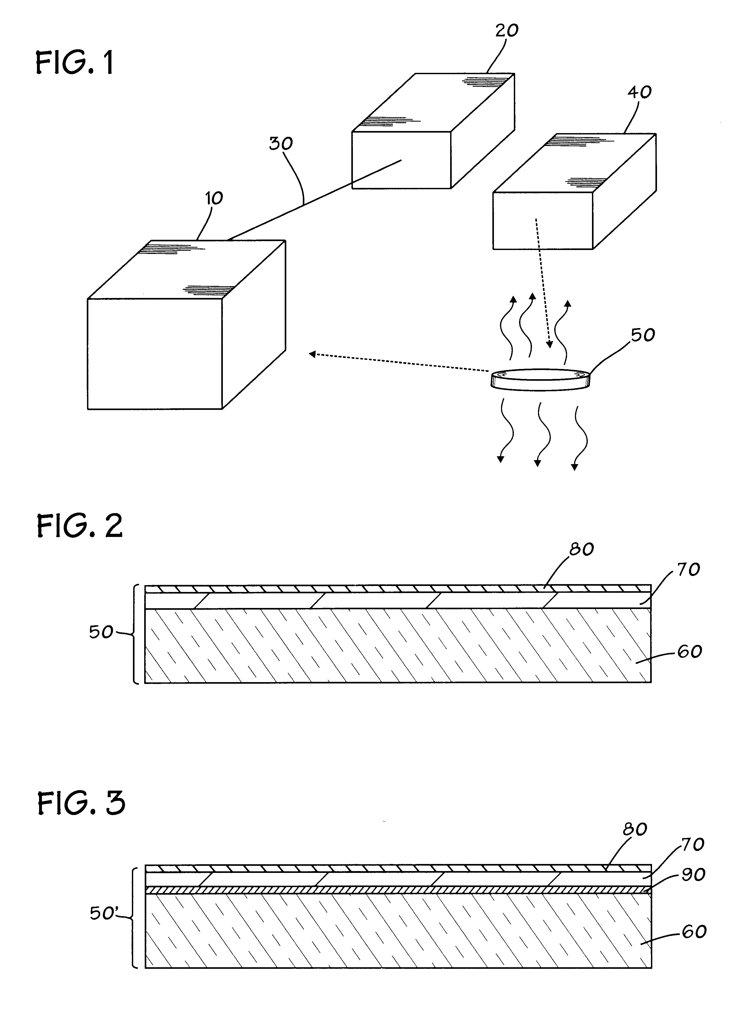
In the drawings described below, reference numerals are generally repeated where identical elements appear in more than one figure. Turning now to the drawings, and in particular to FIG. 1, therein is shown a pictorial view of an exemplary semiconductor vacuum processing chamber 10 that is connected to a pumping system 20 by means of a fluid line 30. A heating or degassing chamber 40 is provided for heating one or more conditioning wafers or workpieces 50. In accordance with the present invention, the heated conditioning wafer 50 is inserted into the processing chamber 10 to aid in the removal of gaseous phase contaminants therefrom and thus increase the vacuum level therein.

In accordance with the present invention, the processing chamber 10 may be a metal PVD chamber, a CVD chamber or virtually any other processing chamber wherein a vacuum is desirable to facilitate the processing. The fluid line 30 is a schematic representation of the connection between the processing chamber 10 a...


PUM

PropertyMeasurementUnit
thickaaaaaaaaaa
thicknessaaaaaaaaaa
pressureaaaaaaaaaa

Abstract

Methods of removing gaseous phase contaminants from a processing chamber, such as a PVD chamber, are provided. In one aspect, a method of removing gaseous phase water from a processing chamber is provided that includes placing a heated substrate that has a titanium film in the processing chamber to dissociate a first portion of the gaseous phase water into hydrogen and oxygen and capture some of the oxygen in, the titanium film. The dissociated hydrogen and uncaptured oxygen are pumped from the processing chamber and the substrate is removed from the processing chamber. Pump down times and test wafer consumption may be reduced.

Description

1. Field of the InventionThis invention relates generally to semiconductor fabrication, and more particularly to a method of removing contaminants from a semiconductor vacuum processing chamber.2. Description of the Related ArtMany semiconductor fabrication processes occur in reduced pressure and / or gas flow environments. Examples of such processes are legion, and include techniques such as physical vapor deposition (sputter) ("PVD"), chemical vapor deposition ("CVD") and low pressure dry etching, to name just few. These various low pressure processes are carried out in a processing chamber in one form or another that incorporates one or possibly several types of vacuum systems. In some fabrication process, such as low pressure dry etching, the requirement for high and ultra vacuum regimes is dictated by the necessity for low operating pressures. In others, such as PVD and various CVD processes, the requirement for high vacuum is dictated by the need to remove gaseous contaminants f...

Claims


Application Information

Patent Timeline
Patent Type & Authority Patents(United States)
IPC IPC(8): B08B9/08B08B7/00C23C14/56C23C16/44
CPCB08B7/0071B08B9/08C23C16/4401C23C14/564Y10S438/905
Inventor BRENNAN, WILLIAM S.RIVERA, WILLIE
Owner GLOBALFOUNDRIES INC
Why Eureka
Try Eureka