Method of patterning lead zirconium titanate and barium strontium titanate

a technology of barium strontium titanate and zirconium titanate, which is applied in the direction of basic electric elements, semiconductor/solid-state device manufacturing, electric apparatus, etc., can solve the problem that ferroelectric materials typically exhibit polarization hysteresis

Inactive Publication Date: 2002-08-20
APPLIED MATERIALS INC
View PDF20 Cites 45 Cited by
  • Summary
  • Abstract
  • Description
  • Claims
  • Application Information

AI Technical Summary

Problems solved by technology

In addition, ferroelectric materials typically exhibit polarization hysteresis.

Method used


Image

  • Method of patterning lead zirconium titanate and barium strontium titanate
  • Method of patterning lead zirconium titanate and barium strontium titanate

Examples


example two

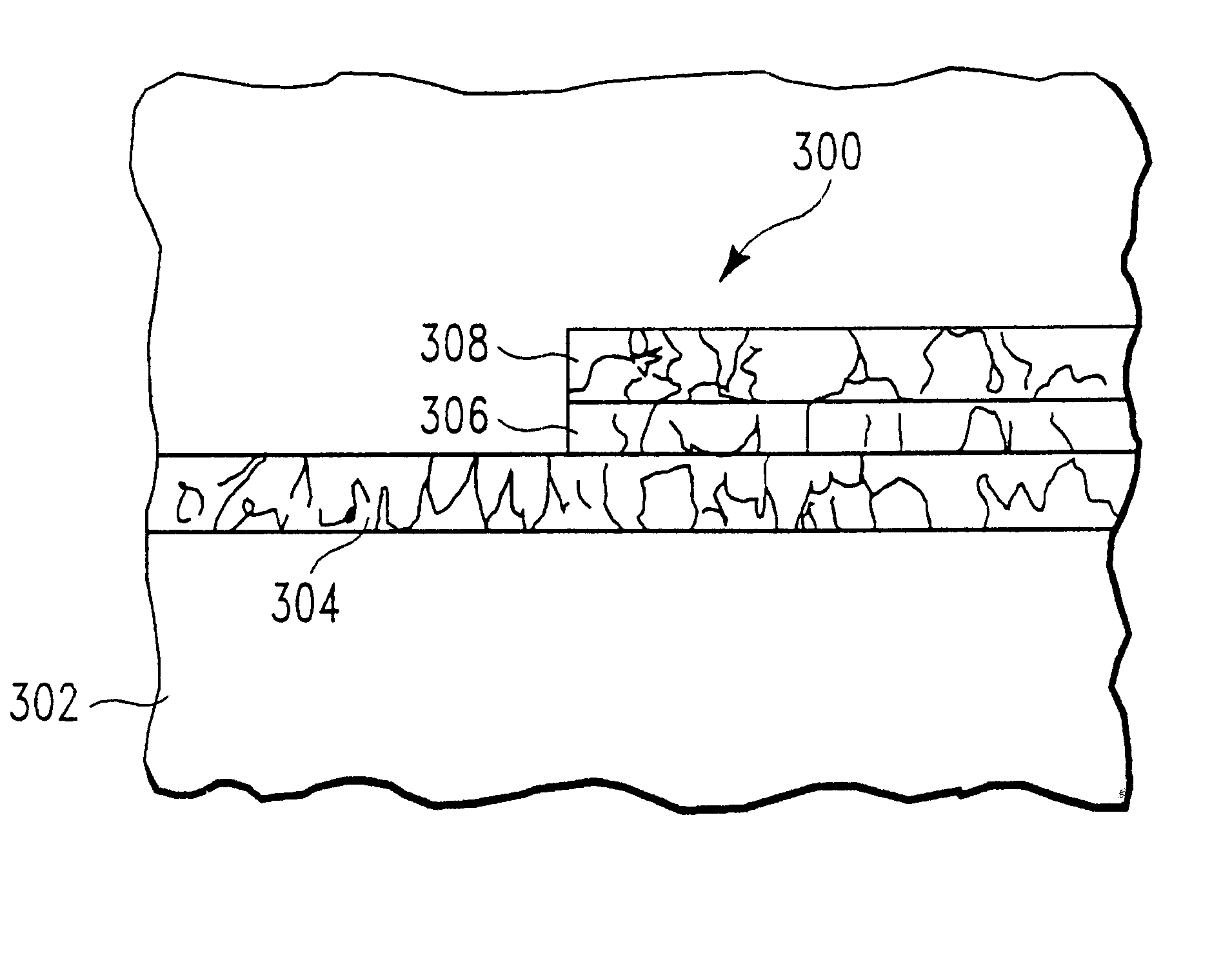
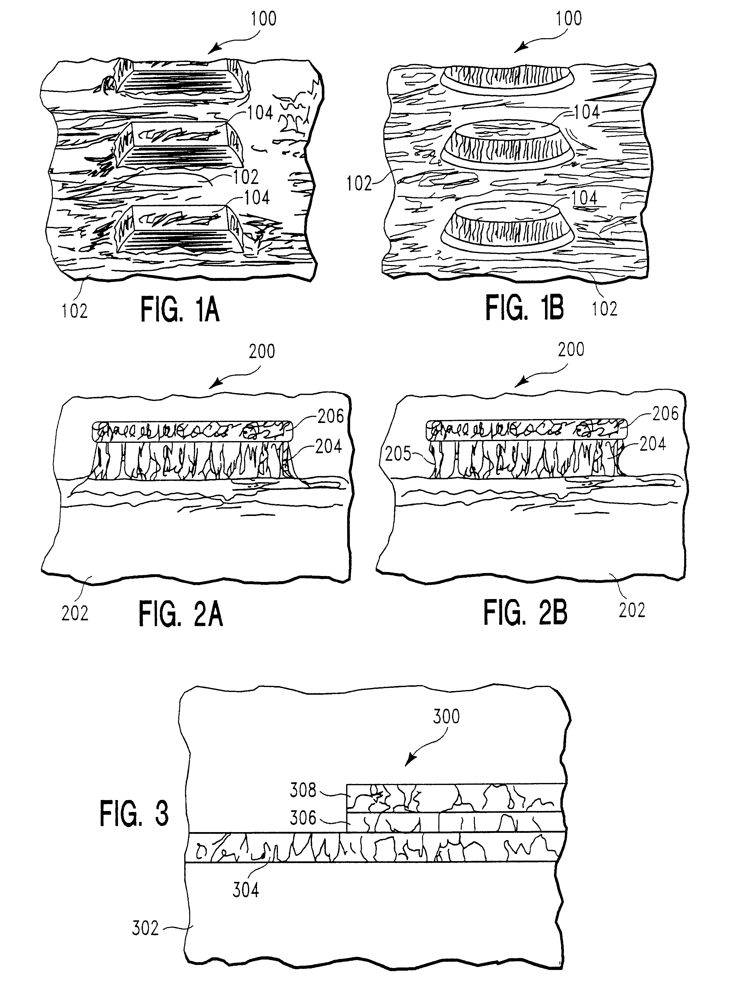
FIG. 3 shows a schematic illustrating a photomicrograph of an etched semiconductor structure 300, formed using the present invention. The etch stack prior to patterning included, from top of the etch stack toward the underlying substrate: an I-line photoresist having a thickness of 1.0 .mu.m (not shown); a masking layer of TiN having a thickness of 1,000 .ANG. (not shown); an upper electrode layer 308 of Ir having a thickness of 1,000 .ANG.; an interlayer 306 of PZT dielectric having a thickness of 1,500 .ANG.; a lower electrode layer 304 of Ir having a thickness of 1,000 .ANG.; and an underlying substrate 302 of SiOx. In this instance, the patterned TiN masking layer (not shown), which was used to transfer the pattern through a portion of capacitor structure including an upper electrode layer 308 of Ir, and interlayer 306 of PZT dielectric, both of which were overlying a lower electrode layer 304 of Ir.

The photoresist patterning was done using methods described in the art. The TiN ...


PUM

PropertyMeasurementUnit
pressureaaaaaaaaaa
temperatureaaaaaaaaaa

Abstract

In an embodiment of the present invention, a method is provided of patterning PZT layers or BST layers. For example, a PZT layer or a BST layer is plasma etched through a high-temperature-compatible mask such as a titanium nitride (TiN) mask, using a plasma feed gas comprising as a primary etchant boron trichloride (BCl3) or silicon tetrachloride (SiCi4). Although BCl3 or SiCl4 may be used alone as the etchant plasma source gas, it is typically used in combination with an essentially inert gas. Preferably the essentially inert gas is argon. Other potential essentially inert gases which may be used include xenon, krypton, and helium. In some instances O2 or N2, or Cl2, or a combination thereof may be added to the primary etchant to increase the etch rate of PZT or BST relative to adjacent materials, such as the high-temperature-compatible masking material. A TiN masking material can easily be removed without damaging underlying oxides. The selectivity of PZT or BST relative to TiN is very good, with the ratio of the etch rate of the PZT film to the etch rate of the TiN mask typically being better than 20:1. In addition, the etch rate for PZT using a BCl3-comprising plasma source gas is typically in excess of 2,000 Å per minute. A substrate bias power is applied to direct ions produced from the BCl3 or SiCl4 toward the surface to be etched. The bias power is controlled to avoid sputtering of a conductive layer or layers in contact with the PZT layer, so that the surface of the etched PZT is not contaminated by a conductive material, which can cause the semiconductor device which includes the patterned PZT to short out.

Description

1. Field of the InventionThe present invention pertains to dynamic and nonvolatile random access memory devices, infrared sensor, and electro-optical devices, for example, which are formed from ferroelectric thin films. In particular, the invention relates to a method of patterning a lead zirconium titanate ferroelectric film, as well as electrode materials which may be in contact with the ferroelectric film.2. Brief Description of the Background ArtFerroelectric materials belong to a class of crystals whose low symmetry engenders a spontaneous polarization along one or more crystal axes. Ferroelectric crystals are characterized by having polarization vectors that can be oriented in two diametrically opposite directions by applying an external electric field. The polarization states in a ferroelectric crystal are due to displacements of positive metallic and negative oxygen ions in different directions. Thermodynamically stable, these states can be switched from one to the other by ...

Claims


Application Information

Patent Timeline
Patent Type & Authority Patents(United States)
IPC IPC(8): H01L21/02H01L21/311H01L21/316H01L21/3065
CPCH01L21/31122H01L21/31691H01L21/02197H01L21/311H01L21/31144
Inventor YING, CHEN TSANHWANG, JENG H.YAMAUCHI, HIDEYUKIPARK, SEAYOULKAWASE, YOHEI
Owner APPLIED MATERIALS INC
Why Eureka
Try Eureka