Method for the production of a monocrystalline layer on a substrate with a non-adapted lattice and component containing one or several such layers

a monocrystalline layer and substrate technology, applied in the direction of crystal growth process, polycrystalline material growth, chemically reactive gas, etc., can solve the problems of weak limit of monocrystalline films, defects at the boundary layer, and reduced film quality

Inactive Publication Date: 2002-10-15
FORSCHUNGSZENTRUM JULICH GMBH
View PDF10 Cites 89 Cited by
  • Summary
  • Abstract
  • Description
  • Claims
  • Application Information

AI Technical Summary

Benefits of technology

The component according to the invention, e.g. a blue diode based upon a sapphire substrate with a monocrystalline GaN layer or a transistor, especially a modulator field-effect transistor (ModFET), has the advantage that the microelectronic or optoelectronic characteristics of the component can be optimally configured in the layers formed without the detrimental effects or damage of threading dislocations. On the one hand, the layer fabricated according to the invention can form the desired end product. It is however foreseeable that this layer formed in

Problems solved by technology

Usually the production of monocrystalline films is strongly limited by the available substrate material or the quality of the film is reduced.
With layer thicknesses which are usually required for components, this relaxation gives rise to defects at the boundary layer between the layer formed and the substrate whereby, however, many defects can run from the boundary layer to the layer surface (so-called threading dislocations).
Since usually these dislocations develop through newly grown layers, they redu

Method used


Image

  • Method for the production of a monocrystalline layer on a substrate with a non-adapted lattice and component containing one or several such layers
  • Method for the production of a monocrystalline layer on a substrate with a non-adapted lattice and component containing one or several such layers
  • Method for the production of a monocrystalline layer on a substrate with a non-adapted lattice and component containing one or several such layers

Examples


example 2

Monocrystalline Si-Ge Mixed Crystal on Si and Subsequent Hydrogen Implantation

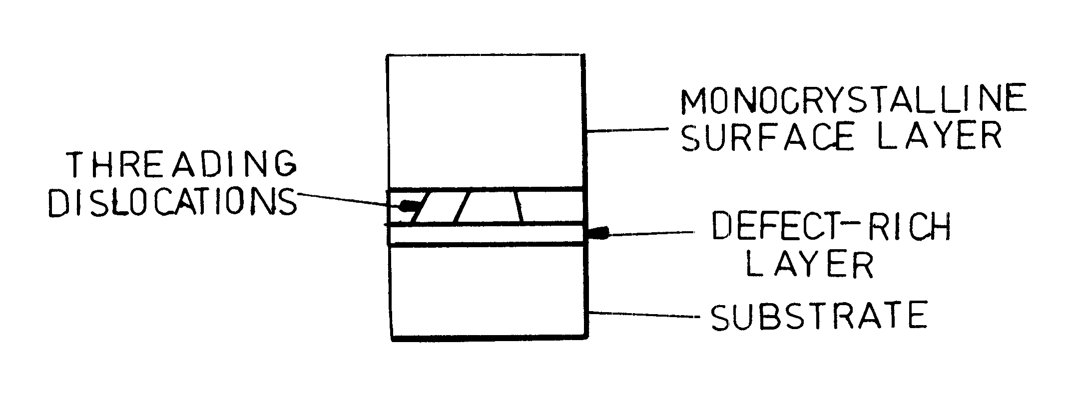
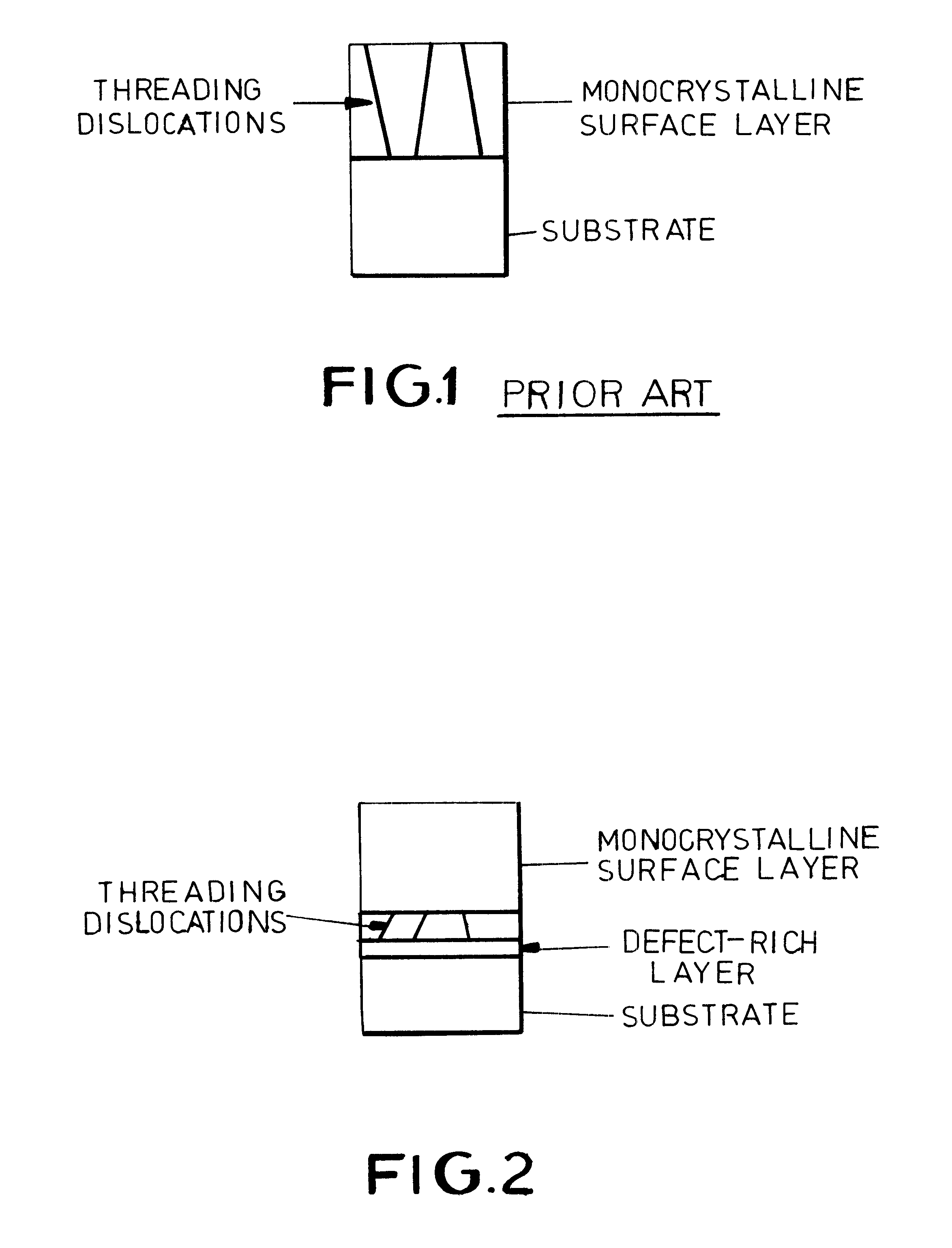
As the substrate, an Si wafer is used. This commercial substrate is cleaned as is customary in Si epitaxy to obtain a perfect and clean surface. Then at 500.degree. C., Si and Ge in a ratio of 80:20 are deposited by means of molecular-beam epitaxy (MBE). The thus obtained monocrystalline surface layer with a thickness of only 200 mm is under mechanical stress. After the epitaxy, the surface layer is implanted with an implantation apparatus with hydrogen with a dose of 1.times.10.sup.16 cm.sup.-2. The implantation energy of the H.sup.+ ions is so chosen, e.g. 20 KeV H.sup.+ that the buried defect-rich layer arises immediately below the boundary layer of the surface film and the Si substrate. By subsequent tempering (100.degree. C., 30 s) the mechanical stress of the surface layer is eliminated, whereby the dislocations run in the buried defect-rich layer in the Si substrate (FIG. 2). The thus produced SiGe ...


PUM


Abstract

The invention relates to a method for the production of a monocrystalline layer on a substrate with a non-adapted lattice. To this end, a monocrystalline substrate with a buried amply defective layer and a monocrystalline layer produce thereon are used. The buried amply defective layer can be produced by hydrogen implantation.

Description

This application is a national stage of PCT / DE99 / 00203 filed Jan. 27, 1999 and based upon German national application 198 02 977.2 of Jan. 27, 1998 under the International Convention.The invention relates to a method of making a monocrystalline layer on an unmatched-lattice monocrystalline substrate in which the monocrystalline layer is formed especially by deposition on the surface of the substrate. The invention further relates to a component containing one or more such layers.Usually the production of monocrystalline films is strongly limited by the available substrate material or the quality of the film is reduced. Different crystal structures as well as different lattice parameters between substrate and layer material (lattice defect matching) limit as a rule a monocrystalline growth of layers of higher quality. An example which is especially important for microelectronic applications is the formation of silicon-germanium (SiGe) alloys on silicon (Si). When monocrystalline laye...

Claims


Application Information

Patent Timeline
IPC IPC(8): C30B23/02H01L21/20H01L21/265H01L21/02
CPCC30B23/02H01L21/0237H01L21/02381H01L21/02532H01L21/02631H01L21/02658H01L21/02694H01L21/26506C30B29/52H01L21/2654
Inventor MANTL, SIEGFRIEDHOLLANDER, BERNHARDLIEDTKE, RALF
Owner FORSCHUNGSZENTRUM JULICH GMBH
Why Eureka
Try Eureka