
Method of heat-treating nitride compound semiconductor layer and method of producing semiconductor device

a technology of nitride compound and semiconductor layer, which is applied in the direction of semiconductors, coatings, semiconductor lasers, etc., can solve the problems of difficult uniform reduction of the resistance of the gallium nitride compound semiconductor layer in the wafer plane, and the long treatment time of the above treatment, so as to achieve the effect of reducing the resistance of the nitride compound semiconductor layer doped with a p-type impurity

Inactive Publication Date: 2003-02-25
SONY CORP
View PDF9 Cites 4 Cited by
  • Summary
  • Abstract
  • Description
  • Claims
  • Application Information

AI Technical Summary

Benefits of technology

It is therefore an object of the present invention to provide a method of heat-treating a nitride compound semiconductor layer in which the resistance of a nitride compound semiconductor layer doped with a p-type impurity can be decreased, and the nitride compound semiconductor layer can be activated, at a far lower temperature than a temperature employed by any conventional method, and a method of producing a semiconductor device by applying the above method of heat-treating a nitride compound semiconductor layer.
In the method according to the third aspect of the present invention, desirably, the lower limit of the heating temperature is at least 200.degree. C., preferably at least 225.degree. C., more preferably at least 250.degree. C., still more preferably at least 300.degree. C. Desirably, the upper limit of the heating temperature is 1200.degree. C. or lower, preferably 700.degree. C. or lower, more preferably 600.degree. C. or lower, still more preferably 500.degree. C. or lower, yet more preferably less than 400.degree. C. When the upper limit of the heating temperature is set at 700.degree. C. or lower, the sharpness of an interface in a superlattice structure is less liable to be disintegrated by the diffusion of atoms (for example, In) constituting the nitride compound semiconductor layer. Further, when the upper limit of the heating temperature is set at 600.degree. C. or lower, further at 500.degree. C. or lower, further at a temperature lower than 400.degree. C., the dissociation of nitrogen atoms from the nitride compound semiconductor layer can be more reliably prevented, and the diffusion of a p-type impurity such as Mg, etc., is less liable to take place. Further, the surface of the nitride compound semiconductor layer is less liable to be oxidized although its degree differs depending upon an atmosphere employed for the heat-treatment.
In the method according to the first, second or third aspect of the present invention, there may be employed a constitution in which a hydrogen-permeable film is formed on the surface of the nitride compound semiconductor layer. In this constitution, examples of a material for constituting the hydrogen-permeable film include so-called hydrogen-occlusion metals such as palladium (Pd) and hydrogen-occlusion alloys. The thickness of the hydrogen-permeable film is not specially limited so long as the dissociation of nitrogen atoms from the nitride compound semiconductor layer by the heat treatment can be prevented. The hydrogen-permeable film can be formed by a physical vapor deposition method (PVD method) such as a sputtering method and a vacuum deposition method or a chemical vapor deposition method (CVD method). For example, a hydrogen-permeable film made of palladium (Pd) is permeable to hydrogen gas at a high temperature, so that it can release hydrogen atoms in the nitride compound semiconductor layer to the heat-treatment atmosphere and can prevent oxidation of the surface of the nitride compound semiconductor layer. Further, palladium can be easily peeled off the nitride compound semiconductor layer and can be also used as a p-side electrode, so that it does not cause the number of steps in the process of producing a semiconductor device, etc., to increase much as compared with the cap layer disclosed in Published Japanese Patent 2540791.
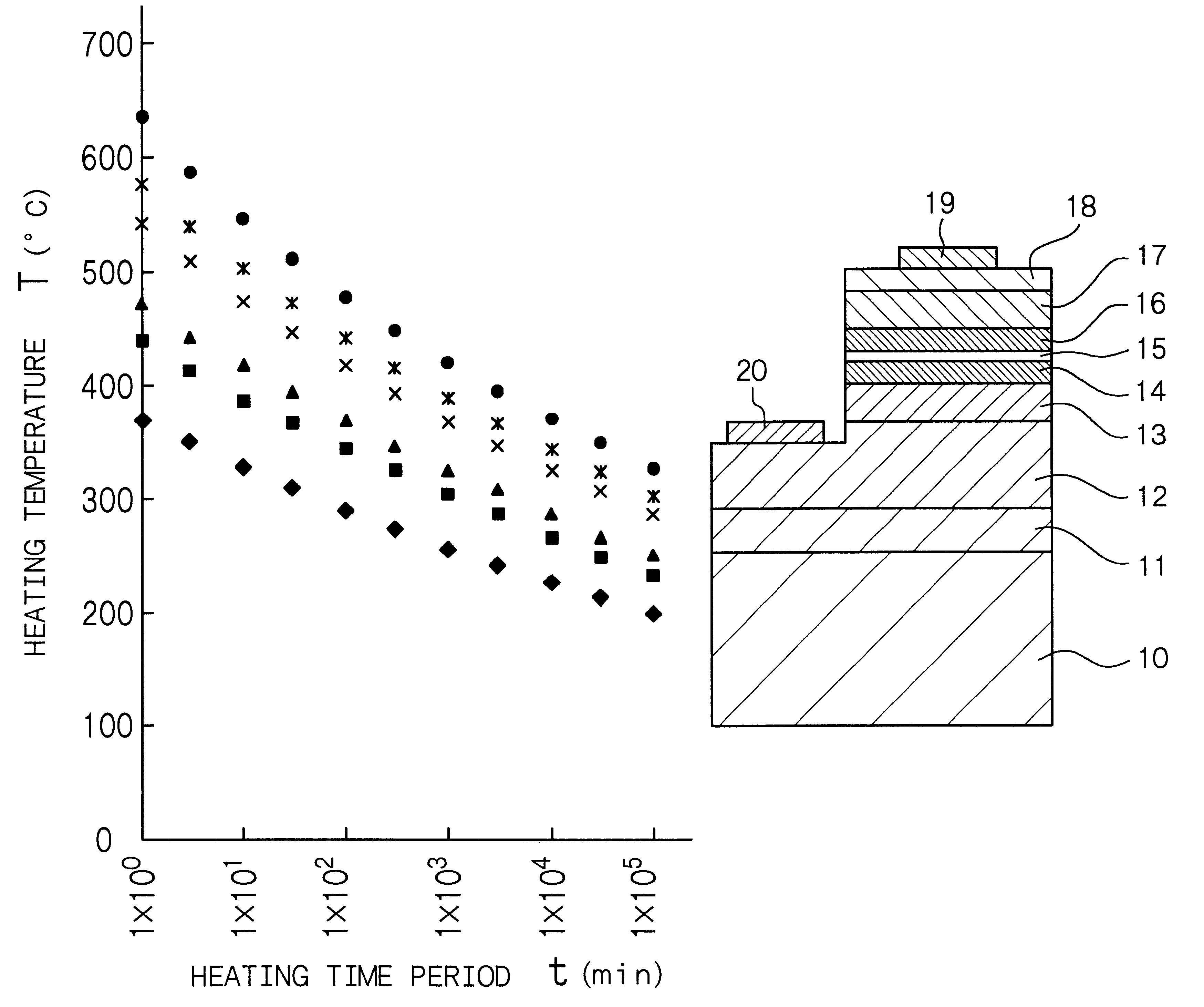
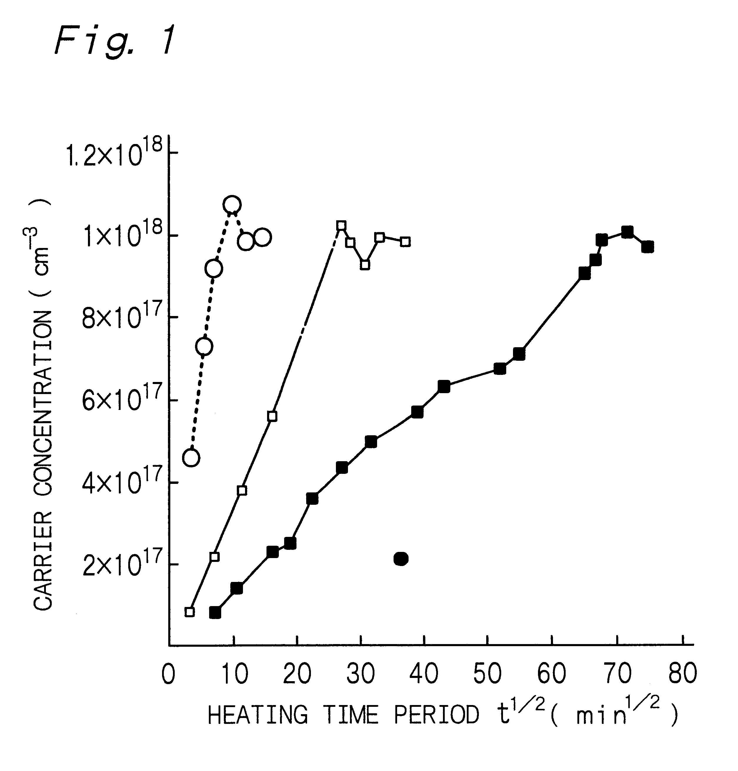
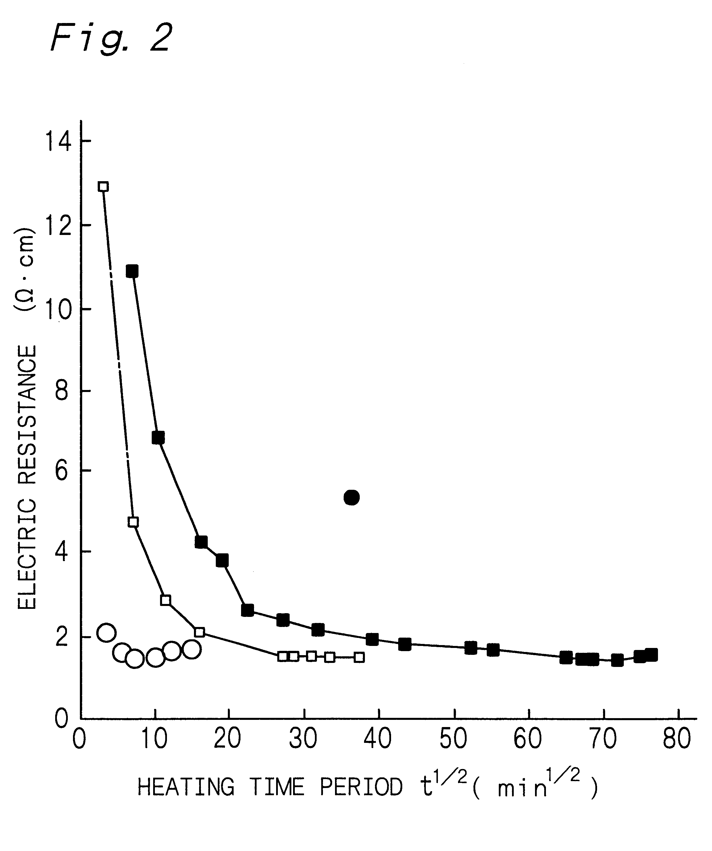
In the method according to the first aspect of the present invention, the heating temperature is set at a temperature that is at least 200.degree. C. but less than 400.degree. C., namely lower than that employed in any conventional method, and the heat treatment is carried out for a longer period of time than that employed in any conventional method, whereby the resistance of the nitride compound semiconductor layer can be decreased and the nitride compound semiconductor layer can be activated. In the method according to the second aspect of the present invention, the heat treatment is carried out under the conditions where the heating temperature T and the heating time period t satisfy t.gtoreq.100 and the equation (1), whereby the resistance of the nitride compound semiconductor layer can be reliably decreased and the nitride compound semiconductor layer can be reliably activated. In the method according to the third aspect of the present invention, the heat treatment is carried out in the atmosphere containing an oxygen gas or containing steam, so that the lower limit of the heating temperature can be decreased as compared with a conventional method. Further, in the method according to the first, second or third aspect of the present invention, the heating atmosphere is selected from aerial atmosphere or an atmosphere supplied at least with an oxygen gas, so that the resistance of the nitride compound semiconductor layer can be decreased and the nitride compound semiconductor layer can be activated for a short heating time period. This is presumably because water, for example, contained in aerial atmosphere works as a kind of catalyst, or oxygen works as a kind of catalyst, on the surface of the nitride compound semiconductor layer during the heat treatment so that the water or oxygen promotes dissociation of hydrogen in the nitride compound semiconductor layer.

Problems solved by technology

In the above method, however, it is only of the surface of the gallium nitride compound semiconductor layer that the resistance can be decreased, and the above treatment takes a long time due to scanning with electron beam.
Further, there is involved a problem that it is difficult to uniformly decrease the resistance of the gallium nitride compound semiconductor layer in a wafer plane.
In production of a semiconductor laser (LD), however, diffusion of a p-type impurity such as Mg is presumably more liable to take place, or the sharpness of an interface in a superlattice structure is presumably more liable to be disintegrated by the diffusion of In with an increase in the heat treatment temperature, and the deterioration of an active layer such as an increase in threshold voltage I.sub.th and a decrease in lifetime is liable to proceed easily.
Further, when the heat treatment is carried out at a high temperature, deterioration takes place in the surface of the gallium nitride compound semiconductor layer due to dissociation of nitrogen atoms.
However, the material for constituting the cap layer is selected from Ga.sub.x Al.sub.1-x N (0.ltoreq.x.ltoreq.1), AlN, Si.sub.3 N.sub.4 or SiO.sub.2, and finally, it is required to remove the cap layer made of such a material from the surface of the gallium nitride compound semiconductor layer, which results in a problem that the number of manufacturing steps increases.

Method used


Image

  • Method of heat-treating nitride compound semiconductor layer and method of producing semiconductor device
  • Method of heat-treating nitride compound semiconductor layer and method of producing semiconductor device
  • Method of heat-treating nitride compound semiconductor layer and method of producing semiconductor device

Examples


example 1

is concerned with the methods of heat-treating a nitride compound semiconductor layer according to the first, second and third aspects of the present invention. Example 1 employed an aerial atmosphere (pressure: atmospheric pressure) as a heating atmosphere.

In Example 1, first, a 40 nm thick buffer layer was formed on a sapphire substrate, then, a 1 .mu.m thick non-doped GaN layer that contained no impurity was formed thereon, and further, a 1 .mu.m thick nitride compound semiconductor layer made of GaN containing Mg as a p-type impurity was formed on the GaN layer. These layers were formed by an MOCVD method. The thus-obtained sample was cut into pieces having dimensions of 5 mm.times.5 mm, and 0.3 .mu.m thick electrodes made of palladium (Pd) were formed on four corners by a vapor deposition method, to prepare test samples for heat-treatment evaluation.

The above test samples for heat-treatment evaluation were placed on hot plates made of stainless steel at T.degree. C. (specifical...

example 2

Example 2 is concerned with the method of producing a semiconductor device that is a semiconductor laser (LD). The method of the above production according to a pressurized MOCVD method that is a kind of a vapor deposition method will be outlined below. In a pressurized MOCVD method, desirably, the MOCVD apparatus for forming various compound semiconductor layers has an internal pressure of 1.1 to 2.0 atmospheric pressures, preferably 1.2 to 1.8 atmospheric pressures. When such a pressurized MOCVD method is employed, there can be reliably prevented a phenomenon that nitrogen is dissociated during the growth of a compound semiconductor layer to cause deficiency of nitrogen in the compound semiconductor layer. In the following explanation, the pressure in the MOCVD apparatus was set at 1.2 atmospheric pressures when various compound semiconductor layers were formed. The pressure in the MOCVD apparatus may be atmospheric pressure. Further, the temperature for forming various compound s...


PUM

PropertyMeasurementUnit
temperatureaaaaaaaaaa

Abstract

A method of heat-treating a nitride compound semiconductor layer, comprising heating a nitride compound semiconductor layer doped with a p-type impurity at a temperature that is at least 200° C. but less than 400° C. for at least 100 minutes.

Description

BACKGROUND OF THE INVENTION AND RELATED ART STATEMENTThe present invention relates to a method of heat-treating a nitride compound semiconductor layer and a method of producing a semiconductor device.In recent years, gallium nitride compound semiconductors such as GaN, an AlGaN compound crystal and an AlInGaN compound crystal are considered promising as component materials for semiconductor devices that can emit light in the range of from a visible light region to an ultraviolet light region. Particularly, since a light emitting diode (LED) using a gallium nitride compound semiconductor has come to be commercially used, the gallium nitride compound semiconductor devices have been of great interest. Further, a semiconductor laser (laser diode, LD) using a gallium nitride compound semiconductor has been reportedly realized as well, and applications thereof including a light source for an optical disk are expected.When a gallium nitride compound semiconductor layer doped with a p-type ...

Claims


Application Information

Patent Timeline
Patent Type & Authority Patents(United States)
IPC IPC(8): H01L21/02H01L21/324H01L33/00C23C16/34H01L21/26H01L21/268H01L21/331H01L29/205H01L29/73H01L33/32H01L33/40H01S5/323H01S5/343
CPCB82Y20/00H01L21/3245H01L33/0095H01S2304/04H01S5/3063H01S5/34333H01L33/325H01L21/324
Inventor TAKEYA, MOTONOBU
Owner SONY CORP
Learn More