Method for fabricating semiconductor device

a semiconductor and device technology, applied in the direction of semiconductor devices, electrical devices, transistors, etc., can solve the problems of restricting the design and fabrication of the device, and reducing the process yield and reliability of the fabrication process, so as to prevent the increase of the junction leakage current, improve the process yield and reliability, and achieve no negative

Inactive Publication Date: 2003-05-13
SK HYNIX INC
View PDF7 Cites 14 Cited by
  • Summary
  • Abstract
  • Description
  • Claims
  • Application Information

AI Technical Summary

Benefits of technology

Accordingly, a method for fabricating a semiconductor device is disclosed which can prevent increase in a junction leakage current and improve a process yield and reliability, by forming a protection film along the rim of the field oxide, forming a SEG layer on the source / drain region, removing the protection film and ion-implanting to form a deep junction in the source / drain region. As a result, the region where the protection film has a deeper junction than the region where the SEG layer is so the ion-implant process has no negative effect on the channel region of CMOS device.

Problems solved by technology

Here, because a N-type-semiconductor field effect transistor (NMOSFET) having a channel on its surface and the PMOSFET have different threshold voltages, there are various restrictions in design and fabrication of the device.
Therefore, a photolithography process should be performed twice, and this complicates the fabrication process.
Accordingly, the device can be easily contaminated due to a wet process, and thus the process yield and reliability thereof are reduced.
In addition, as the sizes of semiconductor devices becomes smaller, the junction depth becomes shallower.
However, in high speed devices, large leakage current occurs due to the salicide process in which silicide layers are formed on the source / drain region and the gate electrode.
However, the conventional method for fabricating the semiconductor device has a limit due to shallow junction region resulting from miniaturization of the device.

Method used


Image

  • Method for fabricating semiconductor device
  • Method for fabricating semiconductor device
  • Method for fabricating semiconductor device

Examples


Embodiment Construction

A method for fabricating a semiconductor device in accordance with preferred embodiments will now be described in detail with reference to the accompanying drawings.

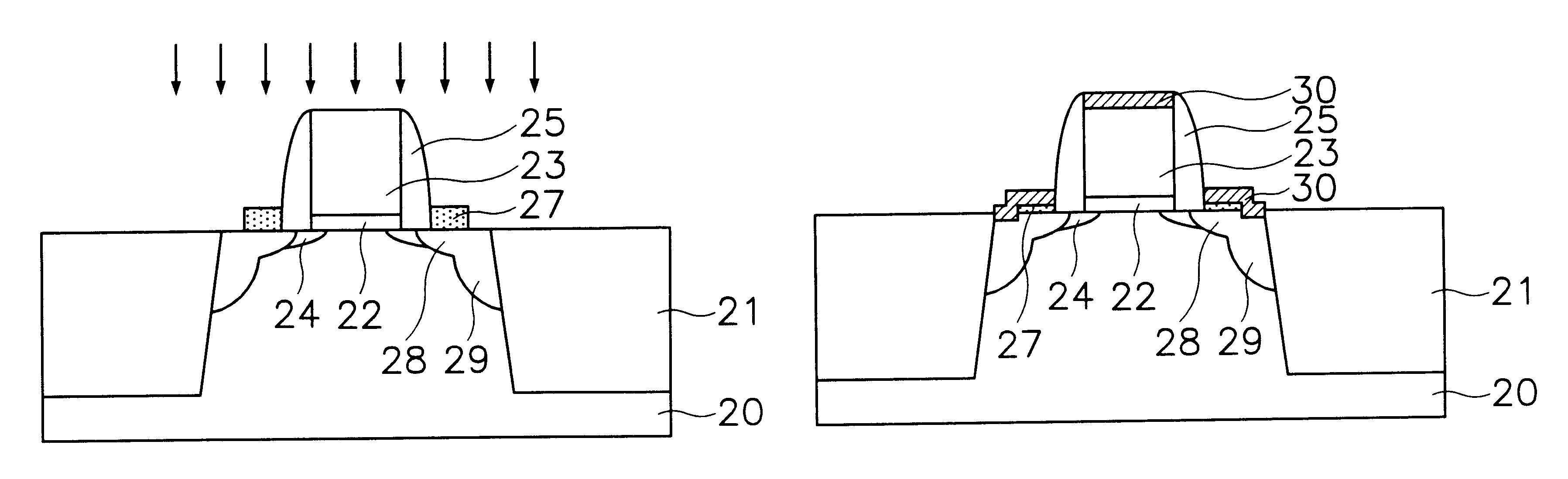
FIGS. 2A through 2D are cross-sectional views illustrating sequential steps of a method for fabricating a semiconductor device in accordance with a first embodiment. A NMOS region or a PMOS region of a CMOS is shown.

First, as shown in FIG. 2B, a field oxide 21 defining an active region is formed on a semiconductor substrate 20. A gate oxide 22 is formed on the semiconductor substrate 20. A polysilicon layer (not shown) is formed on the gate oxide 22. Here, the gate oxide 22 and the polysilicon layer are formed in the NMOS and PMOS regions.

Thereafter, the polysilicon layer is etched using a gate electrode mask as an etching mask, to form a gate electrode 23 in the NMOS and PMOS regions. A first LDD region 24 is formed by ion-implanting a low concentration impurity ions to the semiconductor substrate 20 at both sides of or...


PUM


Abstract

A method for fabricating a semiconductor device employing a salicide (self-aligned silicide) structure is disclosed. The method prevents a junction leakage current from being increased at a portion of a source / drain region which is adjacent to an field oxide, by forming the source / drain region comprised of a relatively deep SID region and a relatively shallow SID region, wherein the deep SID region is formed adjacent to the field oxide and the shallow SID region is formed adjacent to the insulating film spacer. The method comprises the steps of forming a field oxide in a semiconductor substrate, forming a gate oxide and a gate electrode on the semiconductor substrate, forming an LDD region in the semiconductor substrate along a side of the gate electrode, forming a sidewall spacer on each sidewall of the gate electrode, forming a protection layer pattern covering the field oxide and a portion of the LDD region, forming a SEG layer where the protection layer pattern is not covered, removing the protection layer pattern to expose the portion of the LDD region, forming a source / drain region comprised of a deep SID region and a shallow SID region, forming a silicide layer on the gate electrode, the SEG layer and the deep SID region.

Description

1. Technical FieldA method for fabricating a semiconductor device is disclosed. In particular, an improved method for fabricating a high speed semiconductor device is disclosed where the device includes a salicide. In the disclosed method, a shallow and a deep source / drain region are formed simultaneously by forming an insulating film spacer on sidewalls of a gate electrode, forming SEG (selective epitaxial growth) layer in the LDD (lightly doped drain) region adjacent to the insulating film spacer, and then performing an ion implanting process.2. Description of the Related ArtIn general, the most important function of a transistor of a semiconductor circuit is a current driving function. A channel width of a metal-oxide-semiconductor field effect transistor (MOSFET) is adjusted in consideration of the current driving function. In the most widely-used MOSFET, an impurity-doped polysilicon layer is used as a gate electrode, and a diffusion region formed by doping an impurity on a sem...

Claims


Application Information

Patent Timeline
Patent Type & Authority Patents(United States)
IPC IPC(8): H01L21/02H01L29/78H01L21/336H01L29/66H01L21/28H01L21/334H01L21/8238H01L27/092
CPCH01L29/665H01L29/6659H01L29/7834H01L29/66628Y10S438/918H01L21/18
Inventor LEE, HI DEOK
Owner SK HYNIX INC
Why Eureka
Try Eureka