Dual-beam materials-processing system

a material processing system and dual beam technology, applied in the field of dual beam materials processing system, can solve the problems of inability to deposit silicon films directly in high-quality crystalline state, chrome-on-quartz, failure of process, etc., and achieve the effect of reducing fluence through imaging system, prolonging mask life, and high fluen

Inactive Publication Date: 2003-09-16
ANVIK CORP
View PDF7 Cites 96 Cited by
  • Summary
  • Abstract
  • Description
  • Claims
  • Application Information

AI Technical Summary

Benefits of technology

An advantage of the invention is the ability to perform 1:1 image-based materials processing at very high fluence.
is the ability to perform 1:1 image-based materials processing at very high fluence.
Another advantage of the invention is the prolonging of mask life as a result of the reduction in fluence through the imaging system.
Other objects, features and advantages of the invention will be apparent from the following written description, claims, abstract, and the annexed drawings.
References 1. K. Jain, "Scan and Repeat, High-Resolution Lithography System," U.S. Pat. No. 4,924,257, issued May 8, 1990. 2. K. Jain, "A Novel High-Resolution, Large-Field, Scan-and-Repeat, Projection Lithography System," Proc. SPIE, Vol. 1463, p. 666, 1991. 3. K. Jain, "Large-Area, High-Throughput, High-Resolution, Projection Imaging System," U.S. Pat. No. 5,285,236, issued Feb. 8, 1994. 4. K. Jain, "High-Throughput, High-Resolution, Projection Patterning System for Large, Flexible, Roll-Fed Electronic-module Substrates," U.S. Pat. No. 5,652,645, issued Jul. 29, 1997.
(G) BRIEF DESCRIPTION OF THE SEVERAL VIEWS OF THE DRAWING

Problems solved by technology

This is desirable because better-performing thin-film transistor (TFT) devices can be fabricated from crystalline silicon than from amorphous silicon, and it is not possible to deposit silicon films directly in a high-quality crystalline state.
The dual requirements of high fluence and projection imaging with micron-scale patterning present an engineering challenge because the mask materials commonly used, such as chrome-on-quartz, cannot withstand the level of fluence required to melt the silicon films.
If the intensity is too low in particular regions, the film will not melt completely, leading to failure of the process; if the intensity is too high, film damage can occur.
However, it is anticipated that future applications will require a higher level of performance than the SLS-poly microstructure can provide, and no scheme has been conceived for producing microstructures associated with better device performance at high throughput using the conventional SLS equipment.
However, the high fluence at the mask plane poses a serious problem for the implementation of 1:1 imaging for SLS.
The high fluence required to melt the silicon films will damage commonly available mask materials; even the most resistant mask materials currently available are not expected to survive a large number of irradiations at such high fluence.

Method used


Image

  • Dual-beam materials-processing system
  • Dual-beam materials-processing system
  • Dual-beam materials-processing system

Examples


Embodiment Construction

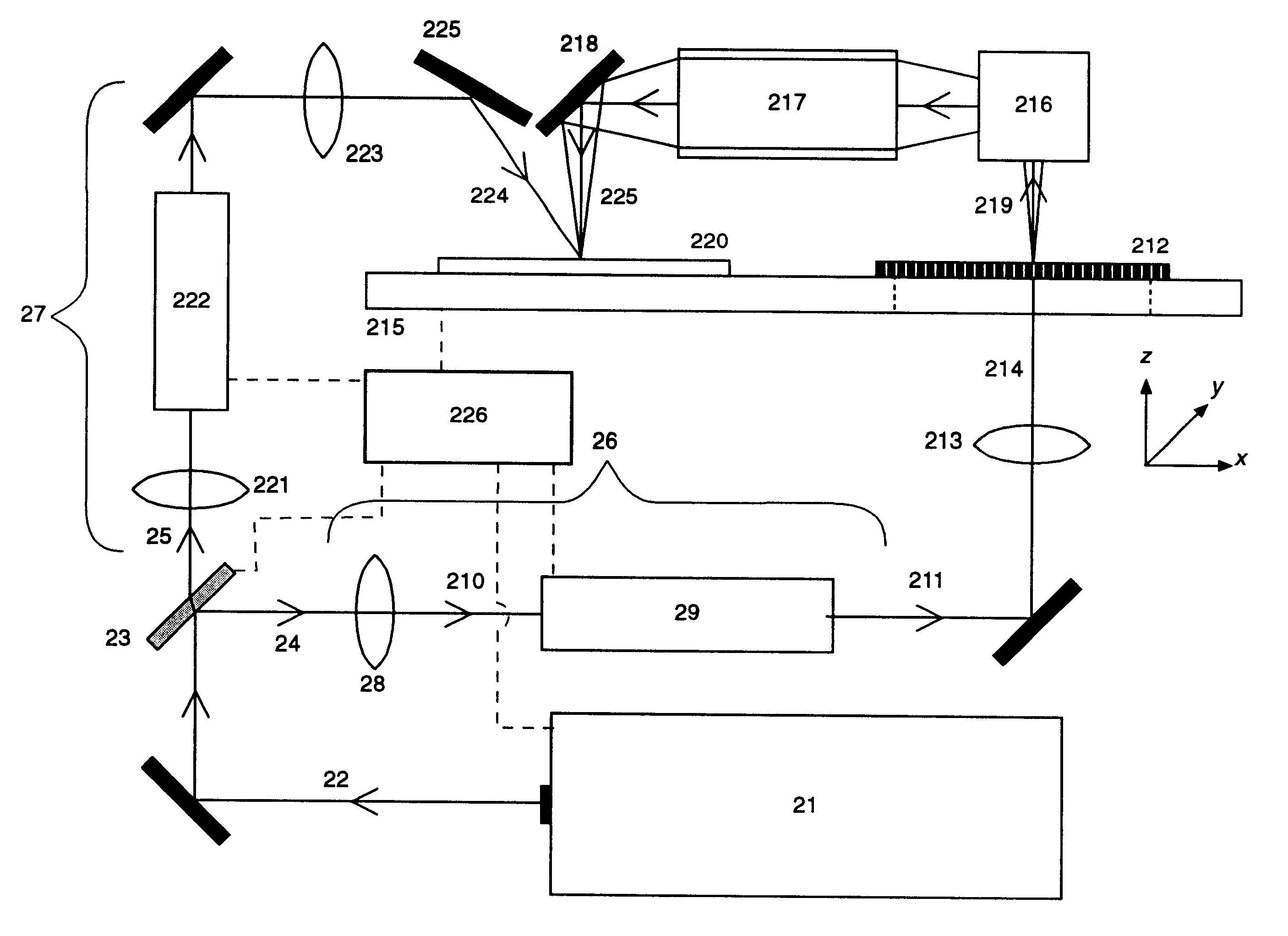
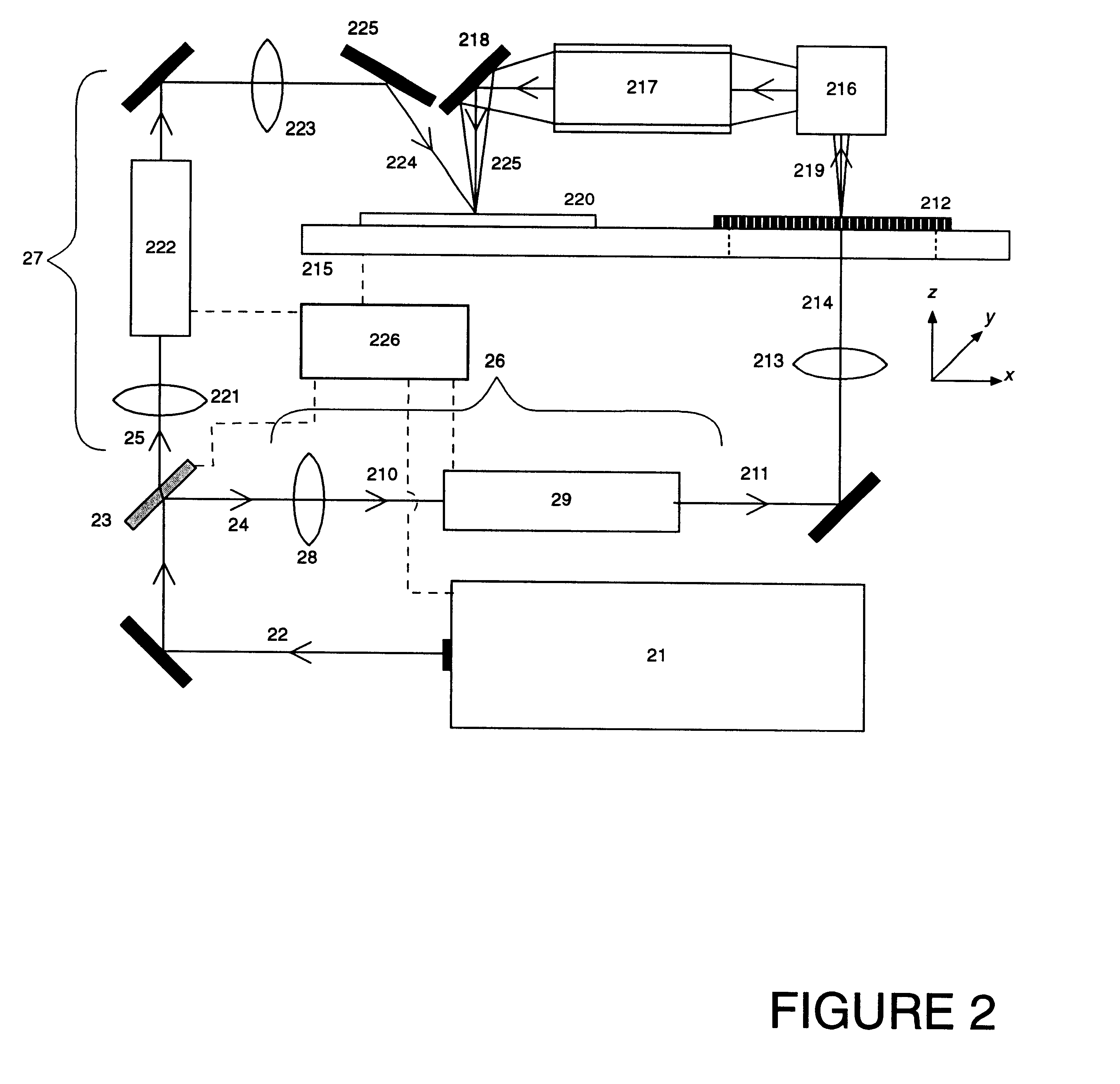
FIG. 2 shows a preferred embodiment of the invention, a high-resolution, pulsed-laser irradiation tool for effecting localized physical changes to a substrate that is based on Anvik's large-area patterning technology: incorporating 1:1 imaging and a single-planar stage. It includes a laser 21, which is preferably a XeCl excimer laser operating at a wavelength of 308 nm with a nominal pulse duration of 30 ns FWHM and a pulse repetition rate that can be varied between one and several hundred pulses per second (Hz). The output beam 22 of the laser 21 passes through a beam-splitter 23, which is preferably a fused silica plate with a multi-layer dielectric coating designed to reflect a fixed portion of the beam, and to transmit the remainder. Beam-splitter 23 divides the laser beam between two optical branches: an imaging branch 24 and a non-imaging branch 25.

There are two illumination subsystems, 26 and 27, for the imaging and non-imaging optical branches, respectively. Each illuminatio...


PUM

PropertyMeasurementUnit
melting pointaaaaaaaaaa
wavelengthaaaaaaaaaa
sizeaaaaaaaaaa

Abstract

Apparatus and method for patterned sequential lateral solidification of a substrate surface, avoiding the need for demagnification to avoid mask damage from fluence sufficient to overcome the threshold for sequential lateral solidification, while using the high throughput of a common stage presenting both 1:1 mask and substrate simultaneously for patterning. The radiation source provides imaging beam and non-imaging beam, each of fluence below the threshold of sequential lateral solidification, but with aggregate fluence above the threshold. The imaging beam path includes a relatively delicate 1:1 mask and 1:1 projection subsystem, with optical elements including a final fold mirror proximate to the substrate surface, put the below-threshold mask pattern on the substrate surface. The non-imaging beam bypasses the delicate elements of imaging beam path, passing through or around the final fold mirror, to impinge on the substrate surface at the same location. Where the radiation patterns of the masked imaging beam and non-imaging beam coincide, their aggregate fluence exceeds the threshold for sequential lateral solidification. The dual selection provides pattern without damage to delicate optical elements.

Description

(B) CROSS-REFERENCE TO RELATED APPLICATIONS(NONE)(C) STATEMENT REGARDING FEDERALLY SPONSORED RESEARCH OR DEVELOPMENT(NONE)(D) REFERENCE TO A MICROFICHE APPENDIX(NONE)(E) BACKGROUND OF THE INVENTION(1) Field of the InventionThis invention relates to a dual-beam materials-processing system for applying two collinear and coincident controlled pulses of radiation to materials for making physical changes; and more particularly, relates to a means for obtaining high-fluence patterned irradiation that is highly uniform, and highly controllable in shape, intensity, and pulse duration to achieve high resolution imaging for materials processing--without feeding a high fluence through the imaging system.(2) Description of Related ArtSeveral techniques have been developed for converting thin amorphous silicon films into polycrystalline films. See Im and Sposili, Materials Research Society Bulletin, 21, 39 (1996). This is desirable because better-performing thin-film transistor (TFT) devices can...

Claims


Application Information

Patent Timeline
Patent Type & Authority Patents(United States)
IPC IPC(8): G03F7/20
CPCG03F7/70216G03F7/70358
Inventor JAIN, KANTISPOSILI, ROBERT S.KLOSNER, MARC A.ZEMEL, MARC I.
Owner ANVIK CORP
Why Eureka
Try Eureka