Enhanced EPROM structures with accentuated hot electron generation regions

a technology of eprom and hot electron generation, which is applied in the direction of semiconductor devices, electrical apparatus, transistors, etc., can solve the problems of sub-threshold voltage degradation, sub-threshold voltage degradation and transconductance degradation, and circuit failures over the life of the circuit, so as to increase the generation of hot electrons, reduce the voltage, and ensure the effect of stability

Inactive Publication Date: 2003-09-16
INTERSIL INC
View PDF16 Cites 21 Cited by
  • Summary
  • Abstract
  • Description
  • Claims
  • Application Information

AI Technical Summary

Benefits of technology

To program the EPROM, the bias conditions are set momentarily so that there is a substantial amount of drain current flowing and hot electrons are generated. Typical bias conditions might be 7.0 volts on the drain and 12.0 volts on the control gate. With these bias conditions, a tremendous amount of hot electrons are generated in a typical 5V, 0.5 micron NMOS transistor. With 12.0 volts on the control gate, there might be 10.0 volts or more across the NMOS gate oxide according to the equation given above. This gate oxide potential "assists" the injection of hot electrons (which already have an abundance of energy) through the gate oxide onto the polysilicon gate. Since the polysilicon gate is a floating gate without connections, these electrons are trapped here due to the oxide insulators which encapsulate the polysilicon once the programming event is completed After .about.200 milliseconds (a typical duration of the programming event), the amount of electrons trapped on the floating gate is significant and sufficient to drastically impact the NMOS transistor characteristics. During such programming, it is possible to increase the NMOS transistor threshold voltage to 4.0-10.0 volts. Assuming this new, higher threshold voltage and the same operating bias conditions described above (5.0 volts on the drain and 2.5 volts on the control gate), the NMOS transistor of the EPROM is now in the "off" state (negligible drain current flowing). By selectively programming EPROMs on a circuit depending on the circuit behavior, the circuit can be trimmed or fine-tuned to enhance its performance. It should be noted at this time that 200 milliseconds to program a single EPROM can be very costly. On a complex circuit, it is possible that several programming iterations must be performed for each circuit which can significantly added to the probe / test cost. A faster programming EPROM could reduce probe / test cost significantly.
Here is the dilemma: special precautions have been taken to control hot electron generation in the standard NMOS transistor, but excessive hot electron generation is desired in the EPROM's NMOS transistor for fast, reliable programming. An improved EPROM semiconductor structure invention is formed by the addition of a P type region that augments a P well doping under a NMOS transistor gate. This added P region under the gate is formed by an additional photolithography and an additional implantation process steps. Alternatively, this P region could be formed during other processing steps that are already in the process flow for other reasons (an NPN transistor P Base, for example). The addition of this new P region changes the dopant grading of the drain-body junction which allows for an increase in the generation of hot electrons in the EPROM NMOS transistor. Hence, the EPROM can be programmed faster and / or at a lower voltage. Only the NMOS transistor of the EPROM receives the added P region. The standard NMOS transistor in the remainder of the circuitry does not have the P region so its reliability is not compromised.

Problems solved by technology

Hot electrons eventually lead to threshold voltage shifts, drive current degradation, sub-threshold voltage degradation and transconductance degradation.
Any or all of these parametric shifts may be sufficient to lead to circuit failures over the life of the circuit.
Hence reliability is compromised.

Method used


Image

  • Enhanced EPROM structures with accentuated hot electron generation regions
  • Enhanced EPROM structures with accentuated hot electron generation regions
  • Enhanced EPROM structures with accentuated hot electron generation regions

Examples


Embodiment Construction

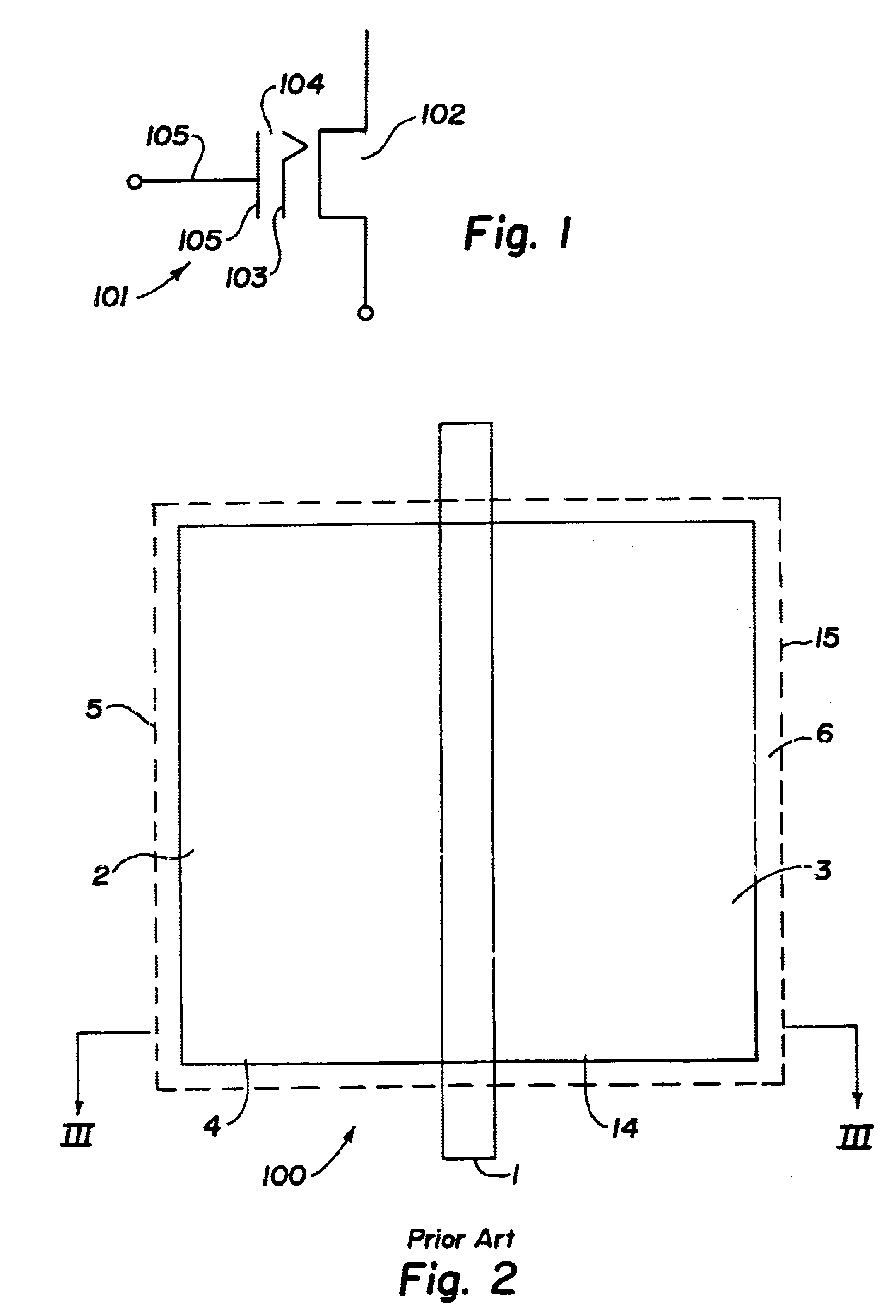
Referring to FIG. 1, there is shown a schematic of an EPROM cell 101 according to the invention. The EPROM cell 101 includes a NMOS transistor 102 integrated with capacitor 104. A control gate 105 is connected directly to one of the plates of a capacitor 104. A floating gate 103 is located between the control gate 105 and the source and drain of transistor 102.

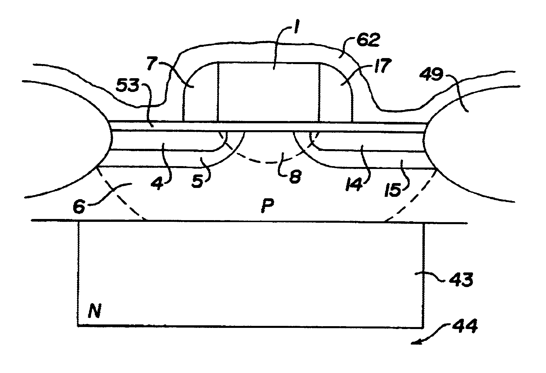
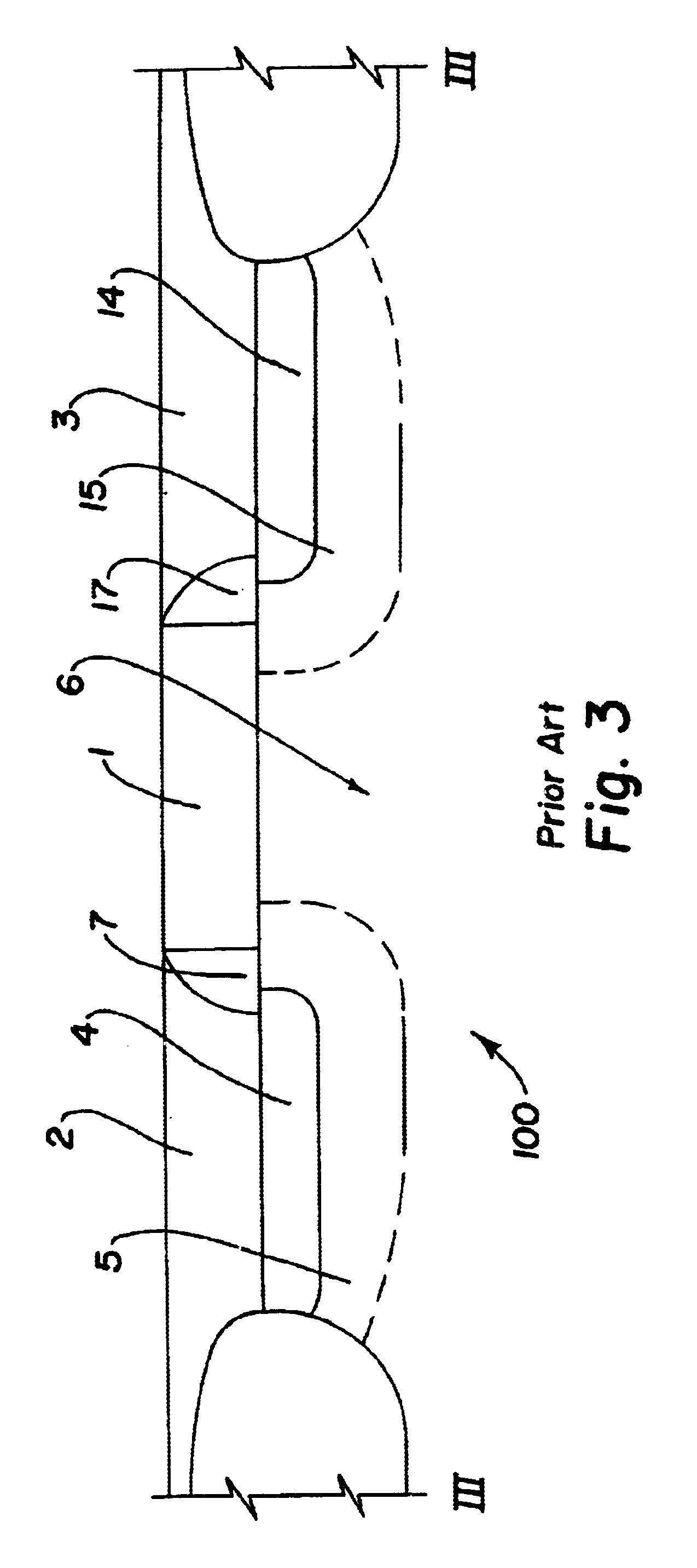
FIGS. 2 and 3 are a top view and a sectional view as seen from lines III--III of a prior art CMOS and BICMOS device structures 100 manufactured on a silicon substrate. The CMOS and BICMOS device structures 100 includes a poly gate 1, a drain 2, and a source 3. The drain 2 and source 3 each include a N.sup.+ region 4 and 14 on the surface of a P well 6. Oxide spacers 7 and 17 are located between the source 3 and drain 2 and around the poly gate 1. Dopant grading is provided between the P well 6 and the N.sup.+ region 4 and 14 of the source 3 and drain 2 by lightly doped drains (Nldd) 5 and 15.

This grading is necessary for relia...


PUM


Abstract

An EPROM structure includes a NMOS transistor integrated with a capacitor. The terminal names of the NMOS transistor follow the conventional nomenclature: drain, source, body and gate. The gate of the NMOS transistor is connected directly and exclusively to one of the capacitor plates. In this configuration, the gate is now referred to as the "floating gate". The remaining side of the capacitor is referred to as the "control gate".

Description

This invention relates to improved EPROM structures and the method of manufacturing the structures with CMOS and BICMOS technologies that utilize lightly doped drain extensions.The prior art CMOS and BICMOS device structures often consist of an N type lightly doped drain (Nldd) which is used to grade the drain to body doping. This grading is necessary for reliability purposes. Without the grading, the drain to body electric field is large enough to generate an abundance of hot electrons. Hot electrons eventually lead to threshold voltage shifts, drive current degradation, sub-threshold voltage degradation and transconductance degradation. Any or all of these parametric shifts may be sufficient to lead to circuit failures over the life of the circuit. Hence reliability is compromised.Attempts have been made to solve this problem. U.S. Pat. No. 4,970,565 dated Nov. 13, 1990, describes a method of building a sealed charged storage structure in a memory cell for an EPROM device which is...

Claims


Application Information

Patent Timeline
Patent Type & Authority Patents(United States)
IPC IPC(8): H01L21/02H01L21/28H01L21/336H01L29/66H01L29/788
CPCH01L21/28273H01L29/66825H01L29/7885H01L29/40114
Inventor CHURCH, MICHAEL DAVID
Owner INTERSIL INC
Why Eureka
Try Eureka