Self alignment process to fabricate attenuated shifting mask with chrome border

Inactive Publication Date: 2003-10-07
TAIWAN SEMICON MFG CO LTD
View PDF7 Cites 18 Cited by
  • Summary
  • Abstract
  • Description
  • Claims
  • Application Information

AI Technical Summary

Benefits of technology

is to provide a method of creating an attenuated phase shifting mask that re

Problems solved by technology

For sub-micron metal line sizes, these highlighted processing steps encounter a number of problems that are typical of device sub-miniaturization.
These problems are problems of poor step coverage of the deposited metal (the metal should be evenly deposited and should fill the profile for the metal line with equal metal density), problems of etching (using dry etching, but metal such as copper and gold are difficult to plasma etch) and problems of step coverage and planarization for the overlying layer of dielectric.
Additional problems of creating uniform contact holes arise for application where the density of the array of contact holes varies over a relatively large surface area while these contact hol

Method used


Image

  • Self alignment process to fabricate attenuated shifting mask with chrome border
  • Self alignment process to fabricate attenuated shifting mask with chrome border
  • Self alignment process to fabricate attenuated shifting mask with chrome border

Examples


Embodiment Construction

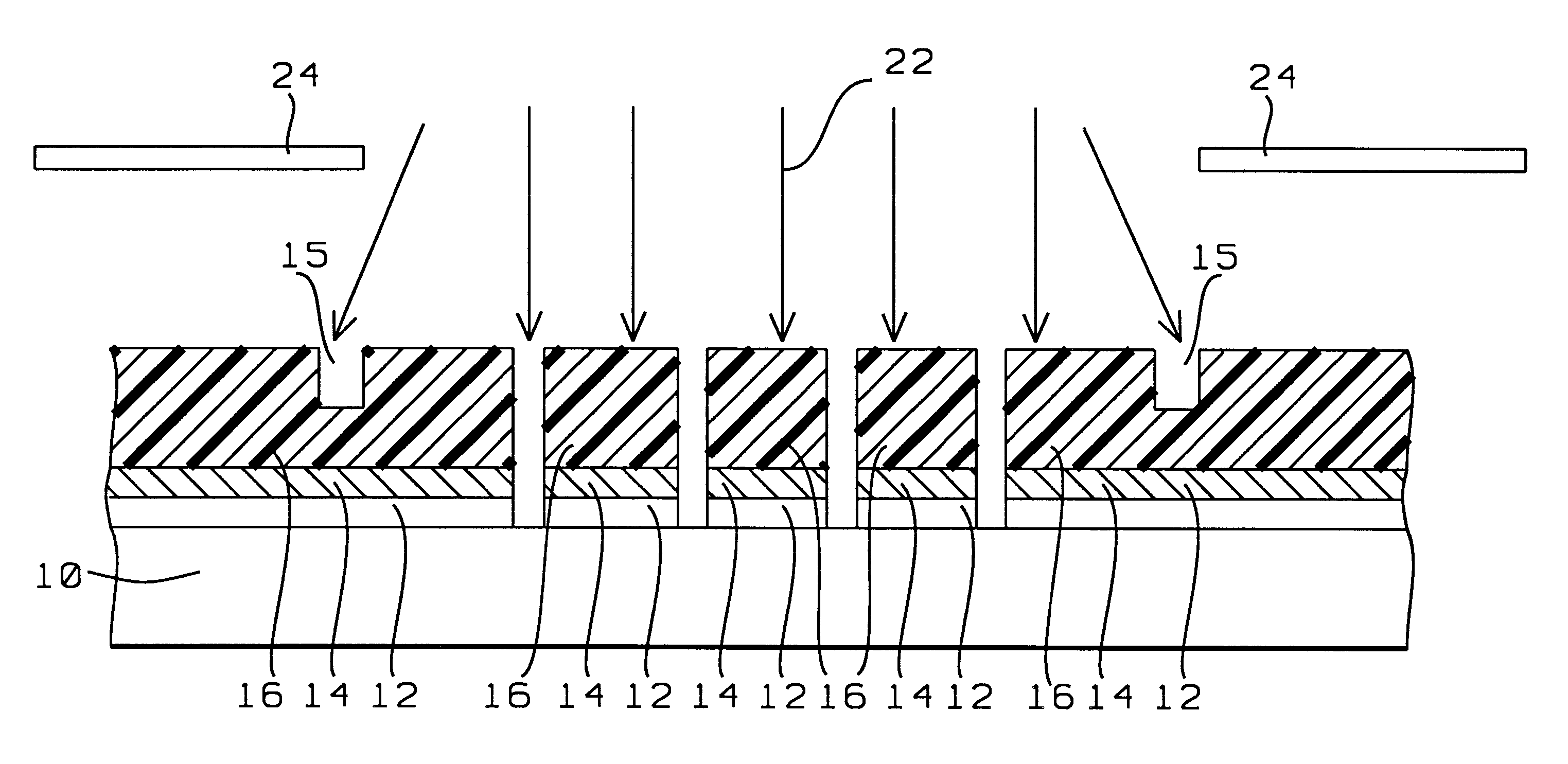
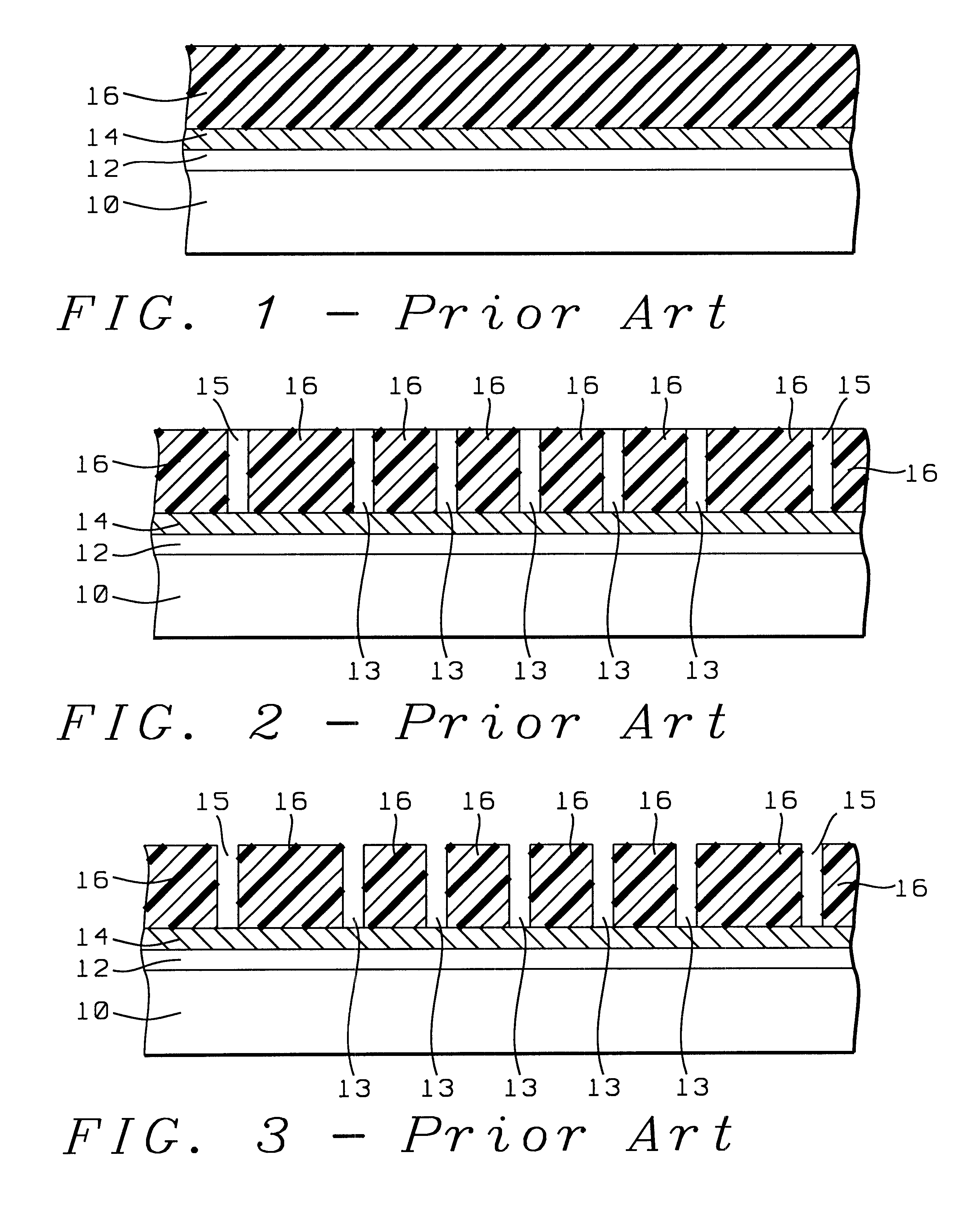
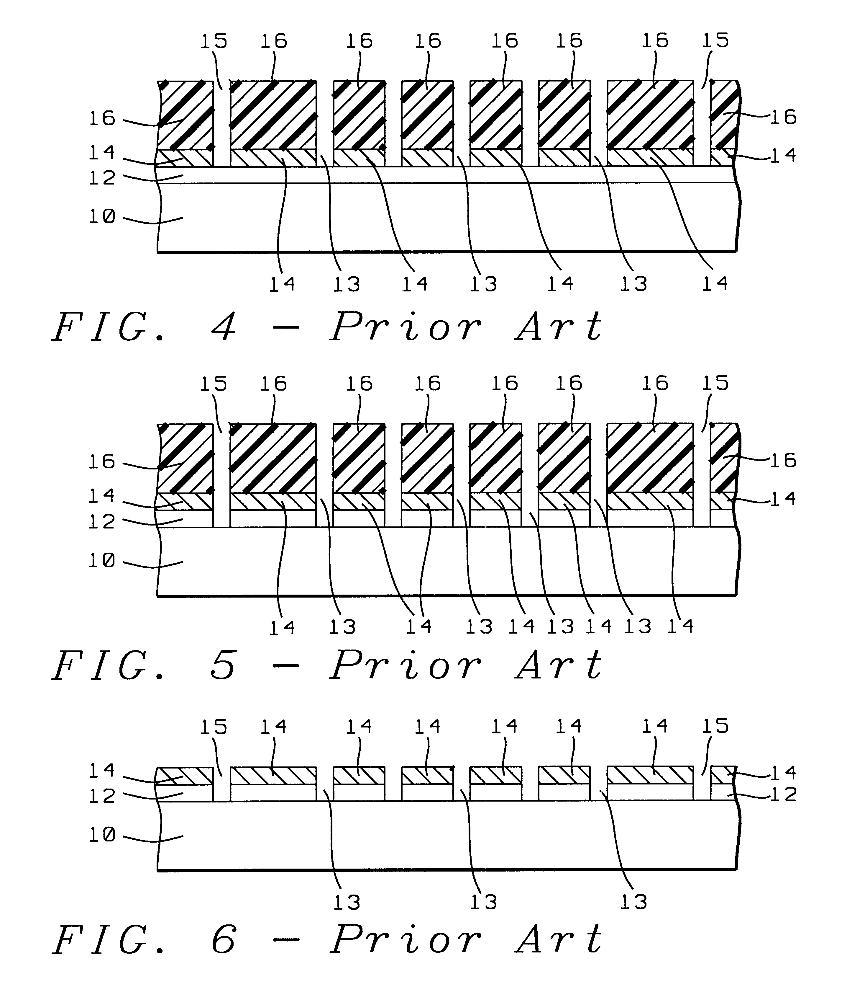
will now be provided by referring to FIG. 1 and to FIGS. 14a and 14b through 21.

FIG. 1 shows a transparent mask substrate 10 that typically is formed of a material such as quartz and to a thickness of about 0.25 inches. A layer 12 of attenuating phase shifting material, such as MoSiON having a thickness of between about 80 and 120 nanometers or CrON having a thickness of between 100 and 140 nanometers is deposited over the surface of the transparent substrate 10. The layer 12 of attenuating phase shifting material has a light transmittance of between about 6% and 10% for light having a wavelength of 365 or 248 or 193 nanometers. A layer 14 of opaque material, such as chrome, has been deposited over layer 12 of phase shifting material to a thickness of between about 80 and 120 nanometers. A layer 16 of photoresist has been deposited over the layer 14 of opaque material. It must be observed at this time that the layer 16 of first photoresist will, under subsequent processing, be expos...


PUM


Abstract

A new method is provided for the creation of an attenuated phase shifting mask. A transparent mask substrate is provided, a layer of attenuating phase shifting material is deposited on the surface of said transparent mask substrate, a layer of opaque material is deposited on the surface of said layer of attenuating phase shifting material. A layer of photoresist is deposited over the surface of the layer of opaque material. The photoresist is exposed by E-beam, creating a mask pattern and a guard ring pattern in the photoresist. The (E-beam) exposed photoresist is removed, the pattern created in the layer of photoresist is used to etch a mask pattern in the layer of opaque material and the layer of attenuating phase shifting material. The remaining photoresist is exposed to UV radiation in the region of the mask pattern and partially in the region of the guard ring. The (UV) exposed photoresist is removed, the remaining photoresist is reduced in height after which the openings of the mask pattern in the opaque layer are increased in size, the outside edge of the guard ring accurately defines the boundary of the device. The remaining photoresist is removed from the layer of opaque material.

Description

(1) Field of the InventionThe invention relates to the fabrication of integrated circuit devices, and more particularly, to a method for the creation of a cost-reduced phase shifting mask whereby further alignment problems that are typically experienced in creating a phase shifting mask are eliminated.(2) Description of the Prior ArtThe manufacturing of semiconductor devices requires the application of multiple diverse technical disciplines that collectively enable the continuing advancement of device performance that has been accomplished since the initiation of the semiconductor device. These various disciplines address various aspects of semiconductor device creation whereby. typically a plurality of active circuits is simultaneously created in a semiconductor substrate. To create a collection of circuits, commonly referred to as Integrated Circuit (IC) devices, the individual circuits are interconnected with metal leads. To further increase device density, multiple layers of int...

Claims


Application Information

Patent Timeline
IPC IPC(8): G03F1/00H01L21/02H01L21/302H01L21/461G03F1/32
CPCG03F1/32Y10S438/942Y10S438/945
Inventor TZU, SAN-DELIN, CHING-CHIA
Owner TAIWAN SEMICON MFG CO LTD
Why Eureka
Try Eureka