Method for the formation and lift-off of porous silicon layers

a technology of porous silicon and lift-off layer, which is applied in the direction of basic electric elements, electrical apparatus, semiconductor devices, etc., can solve the problems of high mechanical strength of separation layer, high cost of soi structure or solar cell, and high cost of soi structur

Inactive Publication Date: 2003-11-18
INTERUNIVERSITAIR MICRO ELECTRONICS CENT (IMEC VZW)
View PDF7 Cites 67 Cited by
  • Summary
  • Abstract
  • Description
  • Claims
  • Application Information

AI Technical Summary

Benefits of technology

The primary aim of the present invention is to provide a novel, one step method for the production of porous layer films. A further aim of the invention is to provide a novel method for the production of porous layer films that allows good control over the pore depth. Another aim of the present invention is to provide a novel method for the production of porous layer films in which the substrate is available without aftertreatment after lift-off of the porous layer film for the production of a further porous layer film.
The method of the present invention can further comprise the step of halting the application of current for a short time, and reapplying the current to obtain a higher thickness of the porous layers. Halting the application of the current will allow the hydrogen to escape before its pressure allows horizontal cracks to occur. By repeating this several time, a porous layer with a desired thickness can easily be obtained.
In a third further embodiment, the method of the present invention further comprises applying a second aqueous solution, suitable for electro-polishing the substrate and for providing separation and lift-off of the low porosity layer and a part of the high-porosity layer from the substrate and for providing a new polished surface on the substrate, while maintaining the current. An alternative way to obtain the same effects is to apply in a further step a higher current, suitable for electro-polishing the substrate and for providing separation and lift-off of the low porosity layer and a part of the high-porosity layer from the substrate and for providing a new polished surface on the substrate, while maintaining the solution. By using this process, the semiconductor substrate surface is polished after removal of the porous layers and thus no aftertreatment of the semiconductor substrate is necessary to proceed to the manufacture of a further porous layer film.

Problems solved by technology

Most of the expensive silicon wafer will only provide mechanical strength to the cell.
This separation layer is a highly porous layer and is mechanically very weak.
All of the above-mentioned procedures for forming a thin porous layer and separating it from the substrate involve multiple steps, some of which are complex.
Each step adds to the cost of the SOI structure or solar cell.

Method used


Image

  • Method for the formation and lift-off of porous silicon layers
  • Method for the formation and lift-off of porous silicon layers
  • Method for the formation and lift-off of porous silicon layers

Examples


example 2

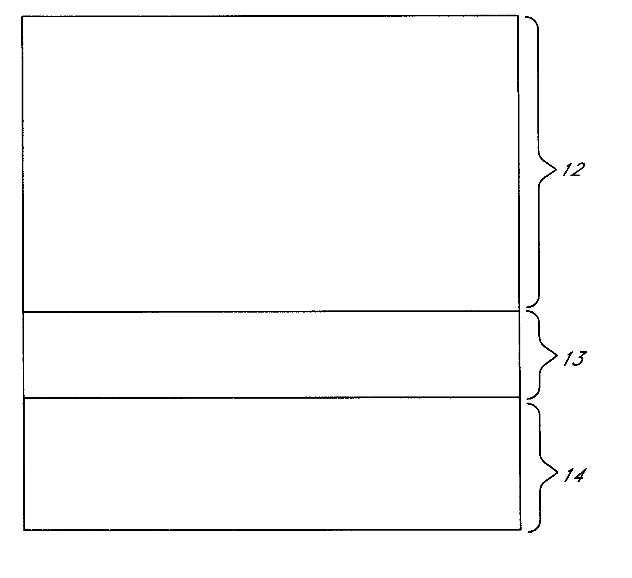
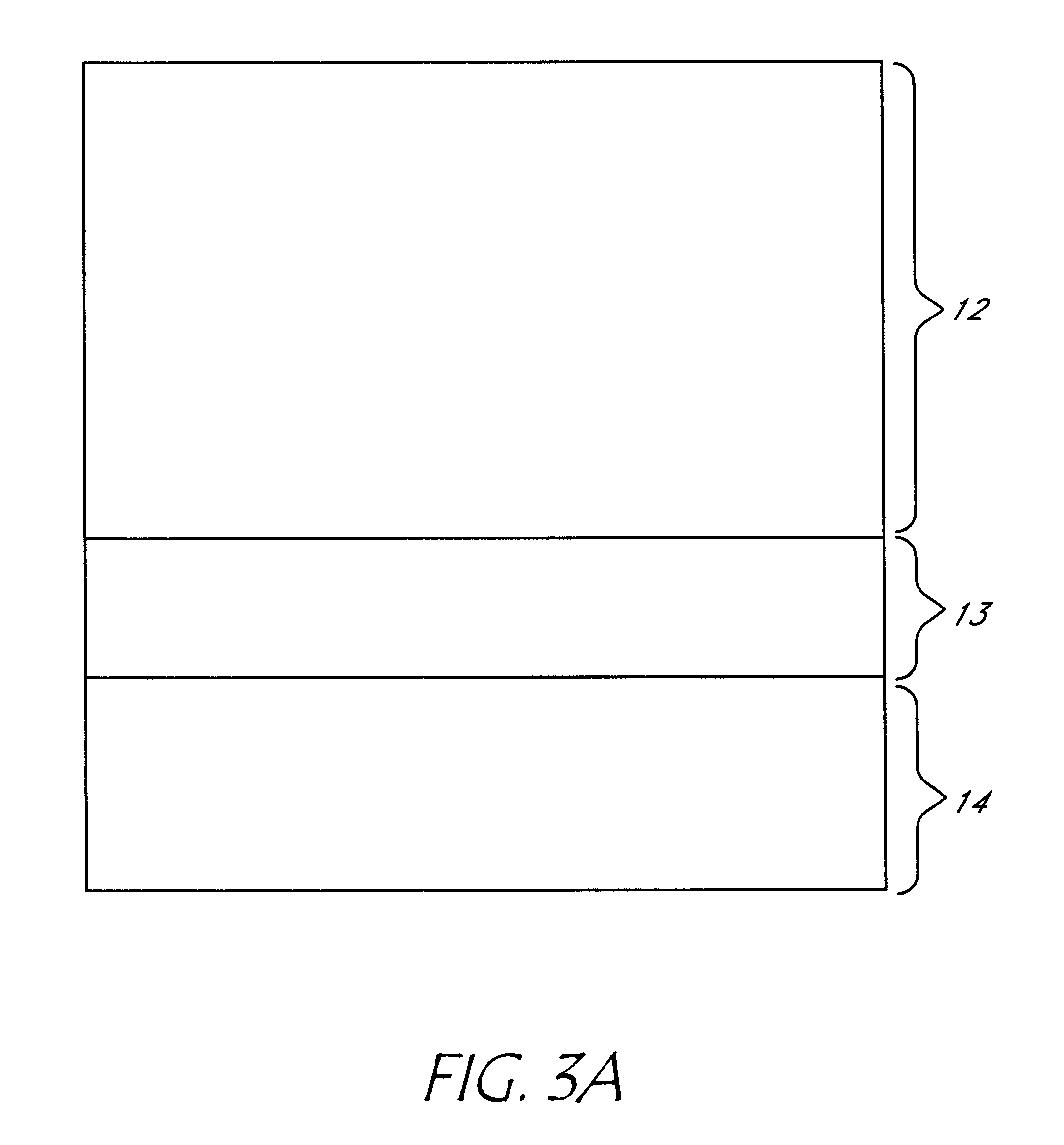
Experiments were carried out with a mixture of HF, acetic acid and deionised water in which the concentration of HF varies between the different experiments from 10% to 40% and current density varies from 25 mA / cm.sup.2 to 200 mA / cm.sup.2. The acetic acid is used as a wetting agent, and provides enough functionality to obtain a good pore distribution. Ethanol could also be used, but for environmental reasons acetic acid is preferred. For a given current density and for a given HF concentration, formation of the separation layer or a very high porosity layer or a detached layer as shown in FIG. 3A is obtained when the reaction is continued after a certain time. The low porosity layer 12, high porosity (separation) layer 13 just before lift-off and silicon wafer substrate 14 are visible on FIG. 3A. For a 25% HF solution and for 150 MA / cm.sup.2 current density this time is around 45-55 second and the thickness of the thin layer obtained is around 7 to 10 microns. Different layer thickn...

example 3

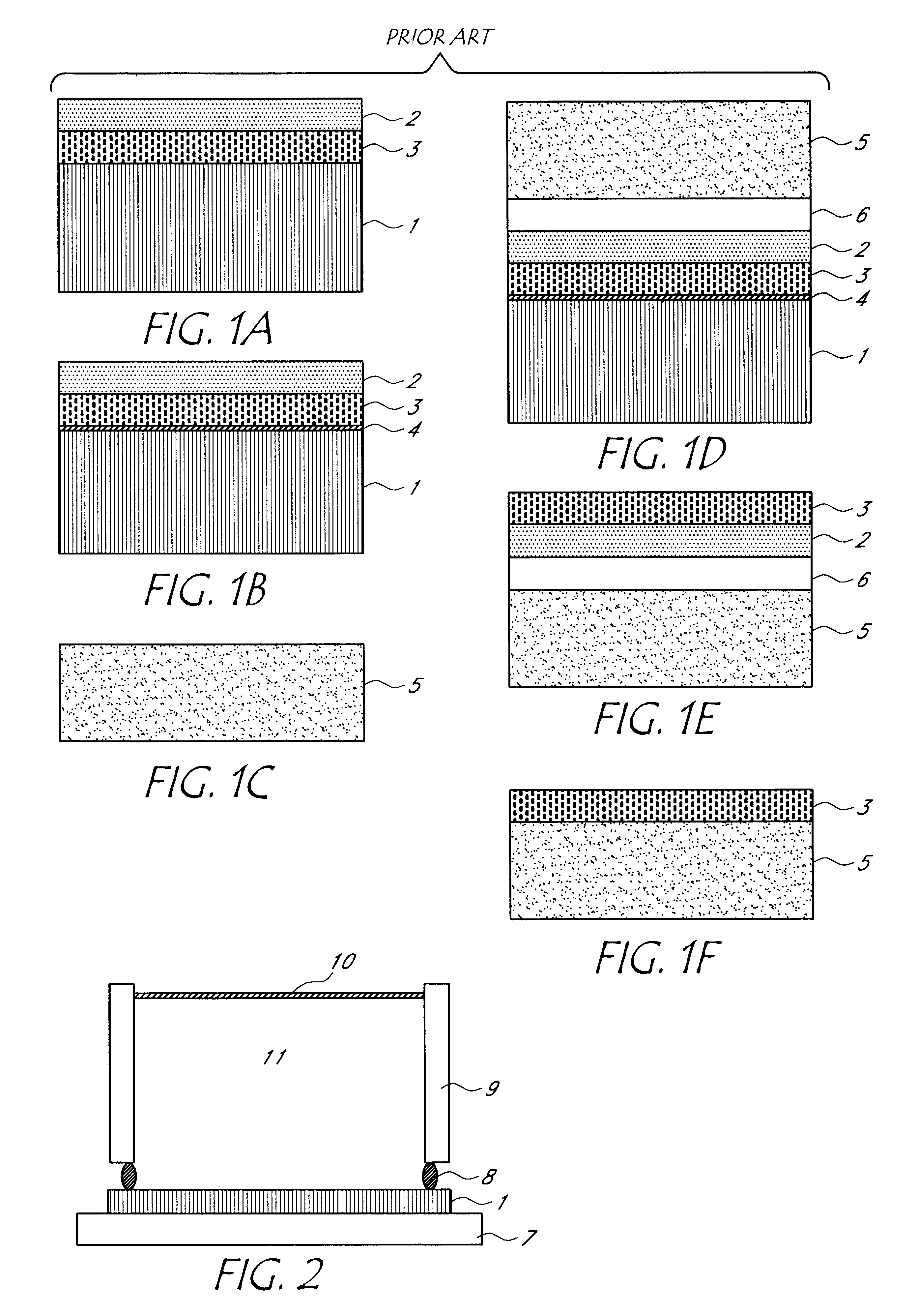
Electrochemical etching of silicon occurs at the HF solution / silicon interface when subjected to the flow of current. When a hole coming from the bulk silicon reaches to the interface, the Si--H bonds is replaced by Si--F bond due to an attack by a fluoride ion from the HF solution. The polarization induced by these Si--F bond lowers the electron density of the Si--Si bond and these are broken too. Silicon dissolves as tetravalent silicon fluoride (SiF.sub.4), which reacts with HF and produces fluorosilicic acid (H.sub.2 SiF.sub.6). This electrochemical reaction is limited to the holes and results in pore formation. FIG. 4 illustrates the interface between bulk silicon and the HF solution where pore formation occurs. The numeral 15 indicates bulk silicon, 16 is the HF solution, 17 designates the holes, 18 are the fluoride ions and 19 is the interface.

Once the pore formation starts at a certain position, it goes straight down in silicon as shown in FIGS. 5A through 5D. The numeral 21...

example 4

For the case of 25% HF solution and 150 mA / cm.sup.2 current density the separation of the PSL occurs at around 45-55 seconds. Because of the high current density, reaction occurs very fast. The centre portion of the layer gets detached with the wafer but the periphery remains attached with the silicon because of the construction of the experimental set-up. Therefore after the formation of separation layer if the reaction is allowed to continue, the by-product, hydrogen, gathers underneath the layer and exerts pressure on the film. The film breaks because of this pressure. Therefore, exact control of the reaction is required.

In another approach, which comprises two steps, one can exploit the use of electro-polishing together with the electrochemical etching for the formation of separation layer. For the purpose of this invention, polishing shall be understood as etching a rough surface such that the uneven topography of the surface decreases. Electrochemical etching is carried out wi...


PUM

PropertyMeasurementUnit
current densityaaaaaaaaaa
thicknessaaaaaaaaaa
current densityaaaaaaaaaa

Abstract

A method for the manufacture, formation, and removal of porous layers in a semiconductor substrate having at least a surface acting as a cathode. The method comprises applying a solution comprising negative Fluorine (F<->) ions between the surface of the semiconductor substrate and an anode. The method further comprises applying a predetermined current between the anode and the cathode. The method further comprises maintaining the predetermined current at substantially the same current value for a sufficient amount of time to obtain a low porosity layer at said surface. A high porosity layer positioned under the low porosity layer is also obtained by the method of the invention.

Description

The present invention is situated in the field of micro-electronics, more precisely in the field of the formation of porous silicon layers (PSL) and its lift-off to manufacture Silicon On Insulator (SOI) structures or to bond it to other low-cost substrates for the fabrication of photovoltaic cells.STATE OF THE ARTWhen manufacturing a solar cell, only the top few microns of a silicon wafer will participate actively in the conversion of solar energy. Most of the expensive silicon wafer will only provide mechanical strength to the cell. This function can be achieved by any other low-cost substrate compatible to the solar cell fabrication process. Thus cost reduction is possible by providing a reduction in the use of silicon.Silicon on insulator (SOI) structures are well known in the art, for example in the manufacture of low-cost solar cells with high efficiency. Some of the advantages are prevention of latch-up, low parasitic capacitance, high-speed operation and the absence of a nee...

Claims


Application Information

Patent Timeline
Patent Type & Authority Patents(United States)
IPC IPC(8): H01L21/70H01L21/02H01L21/3063H01L21/762H01L21/306
CPCH01L21/0203H01L21/76259Y10S438/96
Inventor SOLANKI, CHETAN SINGHBILYALOV, RENATPOORTMANS, JEFBEAUCARNE, GUY
Owner INTERUNIVERSITAIR MICRO ELECTRONICS CENT (IMEC VZW)
Why Eureka
Try Eureka