Laser irradiation apparatus, laser irradiation method, and method for manufacturing a semiconductor device

a laser irradiation and semiconductor technology, applied in metal working apparatus, transistors, manufacturing tools, etc., can solve the problems of extremely low absorption coefficient of laser beam with respect to silicon films, interference with each other, and interference with the above-mentioned interferen

Inactive Publication Date: 2004-02-17
SEMICON ENERGY LAB CO LTD
View PDF11 Cites 114 Cited by
  • Summary
  • Abstract
  • Description
  • Claims
  • Application Information

AI Technical Summary

Problems solved by technology

The cause of the interference patterns seen in the film resides in that the laser beam is split and assembled in 1 region, and therefore the split light brings about interference with each other.
As a result, the influence imparted by the above-mentioned interference to a semiconductor device is extremely small.
The absorption coefficient of this laser beam with respect to silicon films is extremely low, and therefore the laser beam as it is cannot be used in the crystallization process of the a-Si film, which is one of the silicon films.
The largest output of the fifth harmonic is further lower than the aforementioned largest outputs, and thus if the fifth harmonic is used in crystallizing the a-Si film, mass production will become extremely worse.
However, to transform a circular beam into a rectangular linear laser beam is comparatively difficult.
Comparing the energy uniformity of the beam oscillated from the YAG laser which has a beam shape that is circular with that of the excimer laser, the energy uniformity of the former is in general not good.
Thus, a function similar to that of a lens is added to the aforementioned cylindrical crystal rod, thereby worsening the energy uniformity of the beam.
When laser is oscillated at this point in this state, a large amount of light will exit from a side surface of the parallelepiped crystal resulting in a large lost of energy, and thus becoming unusable.
As stated above, the coherent length of the excimer laser is about several microns to several tenths of microns, and therefore the occurrence of light interference when the laser beam passes through the aforementioned optical system, which splits and then converges the laser beam into 1 beam again, is thus very weak.
Hence, the influences of the interference due to this long coherent length of the YAG laser cannot be ignored.
Therefore, the stripes parallel to the linear direction of the linear laser beam eliminate each other out, becoming inconspicuous.
As a problem that occurs when the YAG laser is used in crystallizing the semiconductor film is that interference, as mentioned in the above paragraph, is liable to occur in the YAG laser compared with the excimer laser.
However, in a portion where energy is weak, the energy thereof becomes extremely weak.
Thus, when a region having an immense energy difference is formed, a massive decline in the uniformity of crystallization by using laser is therefore unavoidable.

Method used


Image

  • Laser irradiation apparatus, laser irradiation method, and method for manufacturing a semiconductor device
  • Laser irradiation apparatus, laser irradiation method, and method for manufacturing a semiconductor device
  • Laser irradiation apparatus, laser irradiation method, and method for manufacturing a semiconductor device

Examples


embodiment 1

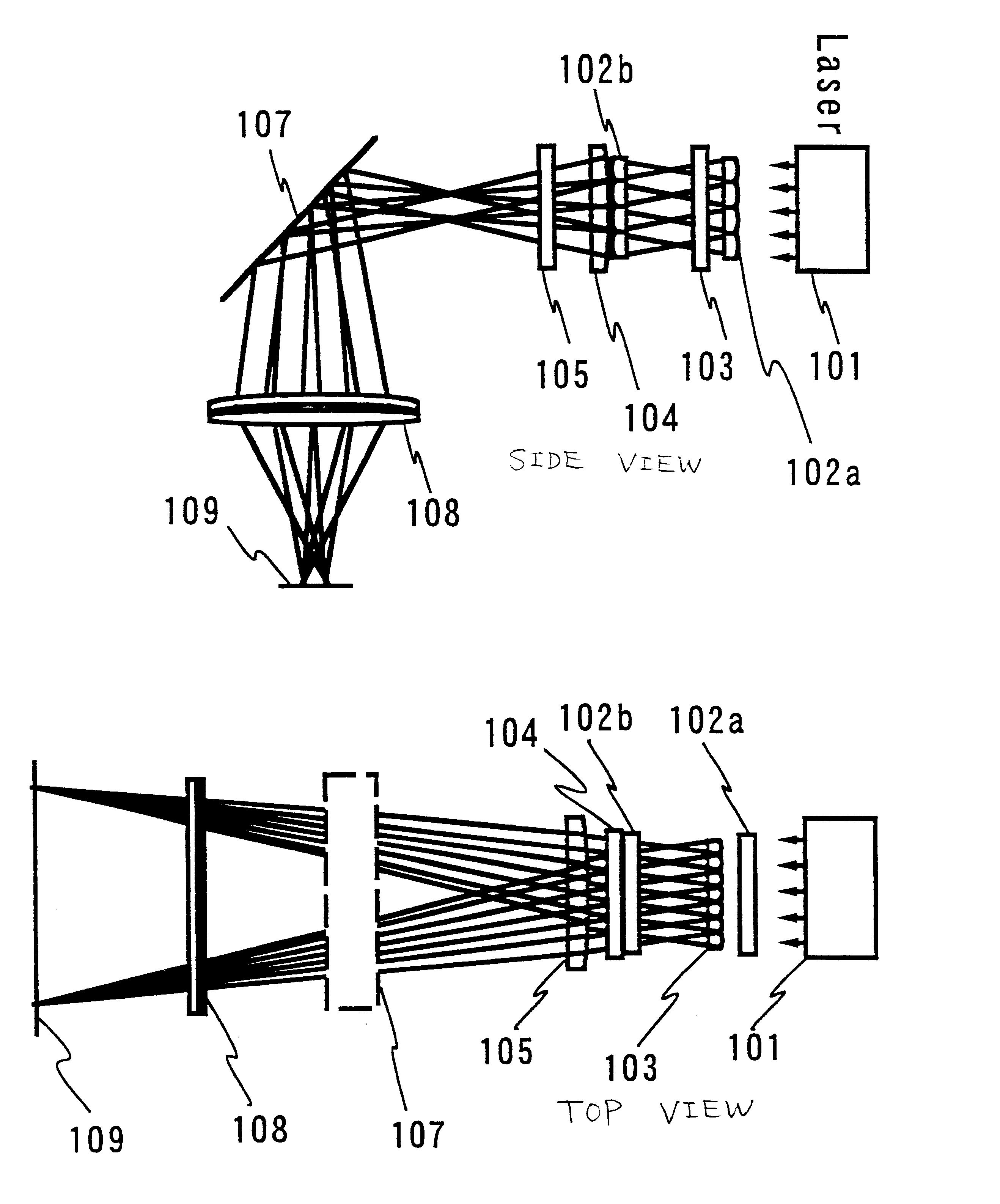
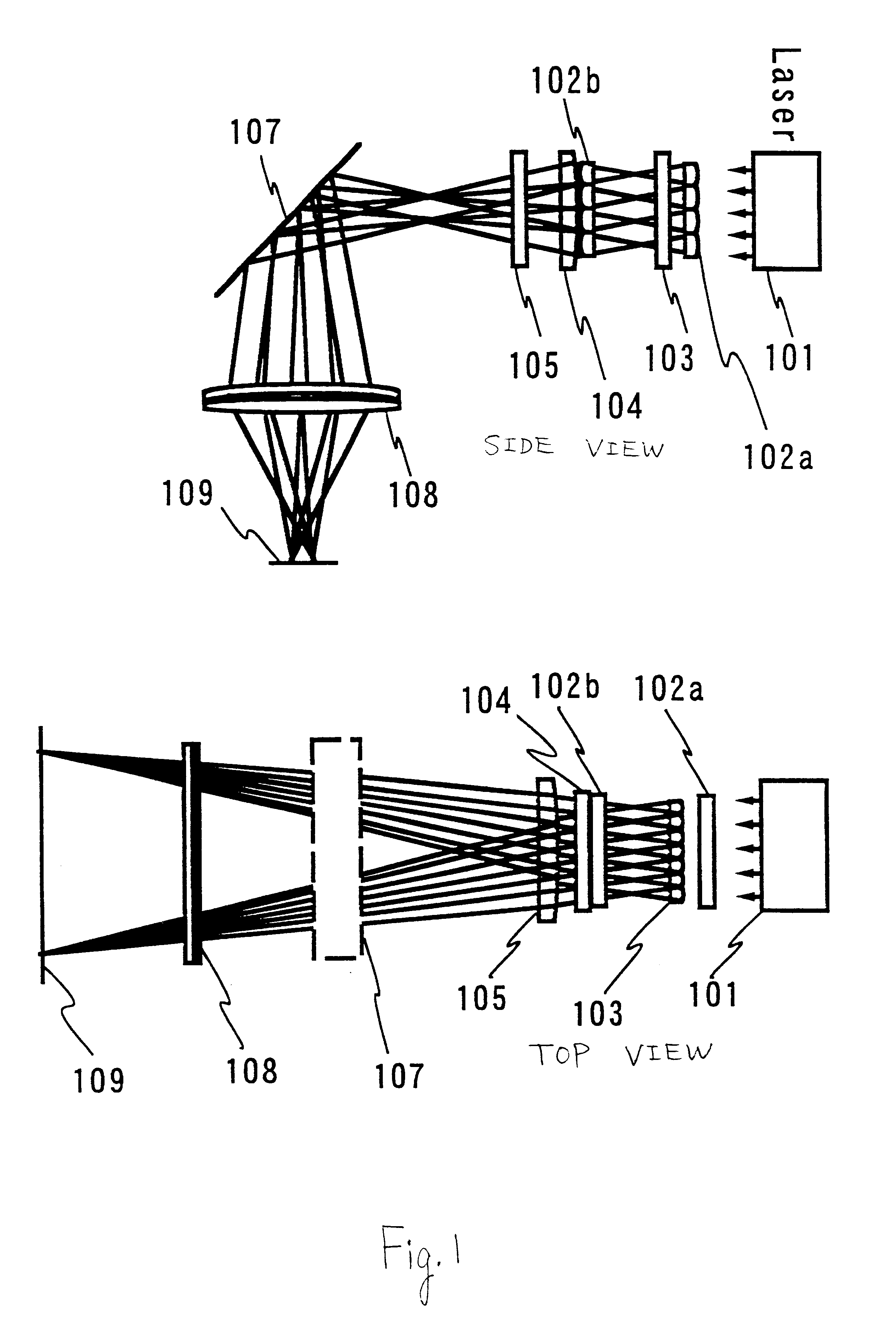
In the present embodiment, an example will be described in which a polycrystalline silicon film is irradiated with a laser beam. The laser irradiation device described in the above embodiment mode is used.

A Corning glass 1737 having a thickness of 0.7 mm is used as a substrate. The substrate has sufficient durability if it is used under 600.degree. C. An SiO.sub.2 film is formed in 200 nm on one surface of the substrate by a plasma CVD method. Further, an a-Si film is formed in 55 nm on the SiO.sub.2 film. Any other film forming method, for example, a sputtering method may be used.

Next, the above-mentioned a-Si film is crystallized by the method disclosed in Japanese Patent Laid-Open No. 7-130652. The method will be described briefly in the following. The above a-Si film is coated with a nickel acetate water solution having a concentration of 10 ppm and then is heated in a nitrogen atmosphere at 550.degree. C. for 4 hours, whereby the a-Si film is crystallized. It is recommended tha...

embodiment 2

can be combined with Embodiment 1.

Embodiment 3

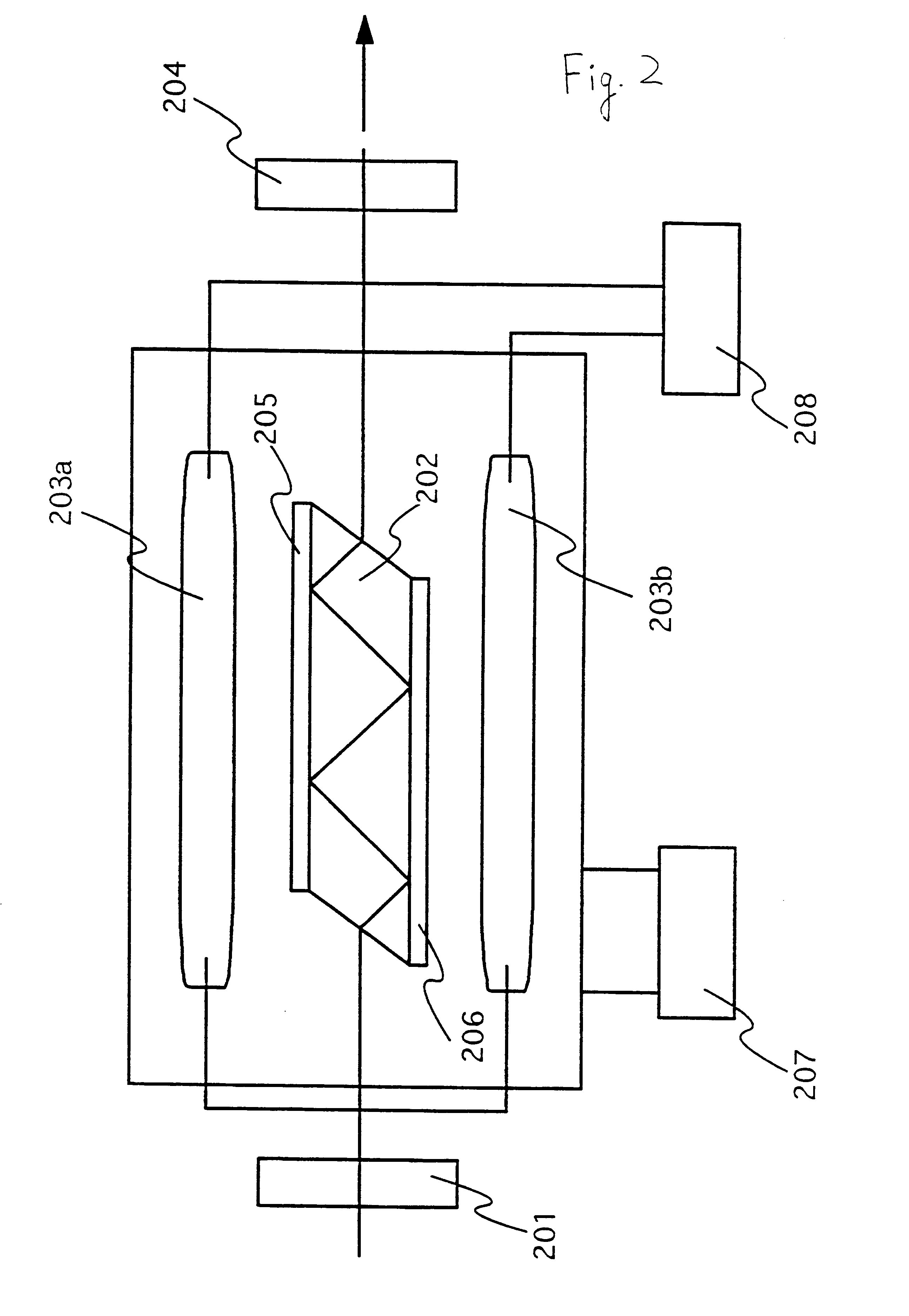
Shown in Embodiment 3 is an example of linearly synthesizing the third harmonic and the fourth harmonic of the YAG laser at the irradiated surface as the light source of the laser beam.

The advantage of using the third harmonic and the fourth harmonic is that both laser beams have an extremely high absorption coefficient with respect to silicon films. By mixing the fourth harmonic with the third harmonic, the influence of interference in the irradiated surface can thus be remarkably reduced.

A method of Embodiment 3 is that a non-linear optical element which forms the third harmonic and the fourth harmonic at the same time is used instead of the non-linear optical element used in the Embodiment Mode of the present invention. Furthermore, a similar optical system for processing the fourth harmonic is used in place of the portion of the optical system, which processes the second harmonic. The fourth harmonic may be entered into the optical s...

embodiment 3

can be combined with Embodiment 1.

Embodiment 4

In the present embodiment, an example of a laser irradiation device for mass production will be described with reference to FIG. 14. FIG. 14 is a top view of a laser irradiation device.

A substrate is carried from a load / unload chamber 1401 by the use of a carrying robot arm 1403 mounted in a transfer chamber 1402. First, the substrate is aligned in an alignment chamber 1404 and then is carried to a pre-heat chamber 1405. In the pre-heat chamber 1405, the substrate is previously heated to a desired temperature of about 300.degree. C., for example, by the use of an infrared lamp heater. Then, the substrate is placed in a laser irradiation chamber 1407 via a gate valve 1406 and then the gate valve 1406 is closed.

A laser beam is emitted by the laser oscillator 1400 described in the embodiment mode and then is bent downward 90 degrees by a mirror (not shown) placed directly above a quartz window 1410 via an optical system 1409 and is transfor...


PUM

PropertyMeasurementUnit
wavelengthaaaaaaaaaa
transmittanceaaaaaaaaaa
thicknessaaaaaaaaaa

Abstract

YAG laser can simultaneously emit a plurality of laser beams having different wavelengths from each other. By simultaneously irradiating the laser beams having different wavelengths from each other to a same region of a non-single crystal semiconductor film, an interference influence is suppressed to obtain a more uniform laser beam. For example, by simultaneously generating second and third harmonics of YAG laser to irradiate the same region through suitable optical system, a laser beam having higher uniformity and having an energy in which interference is highly suppressed is obtained.

Description

1. Field of the InventionThe present invention relates to an apparatus for manufacturing a semiconductor device having a circuit structured with a thin film transistor. For example, the invention relates to an apparatus for manufacturing an electro-optical device, typically a liquid crystal display device, and the structure of electric equipment mounted with such an electro-optical device as a component. Note that throughout this specification, the semiconductor device indicates general devices that may function by use of semiconductor characteristics, and that the above electro-optical device and electric equipment are categorized as the semiconductor device.2. Description of the Related ArtIn recent years, the technique of crystallizing and improving the crystallinity of an amorphous semiconductor film or a crystalline semiconductor film (a semiconductor film having a crystallinity which is polycrystalline or microcrystalline, but is not a single crystal), in other words, a non-si...

Claims


Application Information

Patent Timeline
Patent Type & Authority Patents(United States)
IPC IPC(8): B23K26/067B23K26/00B23K26/08B23K26/06B23K26/18H01L21/336H01L21/20H01L21/70H01L21/02H01L27/12H01L21/84H01L29/66H01L29/786B23K26/073H01L21/268H01L21/77
CPCB23K26/0608B23K26/0656B23K26/0661B23K26/067B23K26/0732B23K26/0738B23K26/08B23K26/0807B23K26/0884B23K26/18H01L21/2026H01L27/12H01L29/66757B23K26/009H01L27/1285B23K2201/40H01L29/78621B23K2101/40B23K26/082B23K26/066H01L21/02592H01L21/02686H01L21/02422H01L21/02678H01L21/02488H01L21/02532H01L21/0242H01L21/02672H01L21/02691
Inventor TANAKA, KOICHIRO
Owner SEMICON ENERGY LAB CO LTD
Why Eureka
Try Eureka