Microdischarge devices and arrays

a technology of micro-discharge devices and arrays, which is applied in the manufacture of electric discharge tubes/lamps, discharge tubes luminescnet screens, instruments, etc., can solve the problems of expensive mounting fixtures, bulky devices, fragile quartz or glass envelopes,

Inactive Publication Date: 2004-02-24
THE BOARD OF TRUSTEES OF THE UNIV OF ILLINOIS
View PDF6 Cites 68 Cited by
  • Summary
  • Abstract
  • Description
  • Claims
  • Application Information

AI Technical Summary

Benefits of technology

The present invention provides microdischarge devices and arrays of microdischarge devices that are inexpensive to manufacture and have electrical and optical characteristics that are superior to previous microdischarge devices. These microdischarge devices and arrays may operate at atmospheric pressure and at voltages of 120V or less, and preferably at voltages of not greater than 100 V. Either direct current (DC) or alternating current (AC) voltages may be applied to the electrodes. The microdischarge devices and arrays of microdischarge devices may also be flexible.
An embodiment of a microdischarge device (not drawn to scale) is shown in FIG. 1. The microdischarge device 100 includes a first electrode 106, a second electrode 104 and a dielectric layer 108 (also called an insulating layer or an insulator) disposed between the first electrode 106 and second electrode 104. A cavity 102 is formed in the insulator 108 and may be additionally formed in either or both of the first electrode 106 and the second electrode 104 such that the openings or holes in each of the first electrode 106, insulator 108, and second electrode 104 are aligned with each other. The cavity 102 preferably has a substantially cylindrical shape to more easily couple to optical fiber, for example, and is formed in a direction transverse to the planes containing the electrodes 104 and 106 and insulator 108. The first electrode 106 and second electrode 104 are both electrically and thermally conductive and a potential difference across the insulator 108 is established by a voltage source 110 connected between the first electrode 106 and the second electrode 104. The potential difference creates a discharge in the cavity 102 when a gas is present. The resulting light has emission spectra that are characteristic of the gas selected. This light is subsequently emitted from at least one end of the cavity 102.
The first electrode 106 and second electrode 104 preferably serve to establish the potential difference across the insulator 108 and thereby energize the microdischarge device 100. Thus, the first electrode 106 and second electrode 104 are fabricated from materials having good electrical and thermal conductivity. The first electrode 106 and second electrode 104 may be planar and may be fabricated from thin layers of conductive material, preferably having a thickness of less than 100 .mu.m, more preferably thicknesses from about 10 .ANG.-10 .mu.m and from 50 .ANG.-5 .mu.m. Common metals that may be used to form the electrodes include copper, aluminum, gold, silver, nickel, and zinc and alloys thereof. Other conductors include polymers containing carbon black and other conducting polymer materials or highly doped crystalline, polycrystalline or amorphous semiconductor films. Alternatively, rather than the electrodes being formed from an optically opaque material, at least one of the electrodes may be fabricated from a solid layer of optically transmissive material that does not significantly absorb light at the wavelength of the discharge, such as indium tin oxide (ITO). Optically transmissive material transmits preferably at least 50% of the light impinging substantially normal to the surface of the material at wavelength emitted by the discharge. More preferably, the optically transmissive material transmits at least 60%, 70%, 80%, 90%, or even 95% of the light impinging substantially normal to the surface of the material at a wavelength emitted by the discharge. The first electrode 106 and second conducting electrode 13 preferably form a cathode and an anode.
The insulator 108 may be a polymer such as polyimide, which has exceptional thermostability and dielectric strength. For example, the breakdown voltage for a polyimide film about 5 .mu.m thick is approximately 1.2 kV, giving a dielectric strength in excess of 10.sup.6 V-cm. Other dielectrics, resins and polymers--for example, oxide and nitride films such as metal oxides, SiO.sub.2, Si.sub.3 N.sub.4 or KAPTON--may be used as long as the material retains its insulation properties at the material thickness required for adequate dielectric strength. Furthermore, multiple films of different materials (having different dielectric constants) may be used to fabricate the insulator in order to improve both individual device and array performance. Tests have shown that a multiple layer dielectric (containing, for example, .about.0.5 .mu.m Si.sub.3 N.sub.4, 0.5 .mu.m SiO.sub.2, and several microns of polyimide) not only improves the voltage-current characteristics of an individual microdischarge device but also makes it possible to realize stable operation of large arrays (for example, 30.times.30) of devices. If, on the other hand, the insulator 108 is a single film of polyimide, for example, it is difficult to operate arrays larger than approximately 5.times.5.
The microdischarge device 100 may be less than 50 .mu.m thick (approximately two one-thousandths of an inch), thus giving rise to a thinner device than is typical of conventional microdischarge devices. One feature of arrays of such devices is that the finished array may be flexible and light. Thus, these arrays are able to conform to various shapes and can, if desired, be rolled into a tube. This feature enhances the portability and utility of microdischarge arrays.
Sealing of the microdischarge cavity while containing the desired gas at the proper pressure may be performed in a number of ways other. One method is to "hard seal" the array of microdischarge electrodes and insulator to a quartz window having a conducting film (such as ITO) or a fine metal grid on one side. The bonding process takes place with the conductor facing the electrode and bonding occurs along the entire perimeter of the electrode and quartz. When completed, this structure is robust and compact, requiring only electrical connections to an appropriate power supply. Another approach using flexible optically transmissive material is to laminate an array of electrode / insulator / electrode (or screen) devices. By laminating a plastic sheet on both sides of the microdischarge array assembly, light generated within the array will be transmitted by the packaging if the laminating sheet material is chosen properly. A phosphor / electroluminescent material may also be included on the screen before sealing.

Problems solved by technology

Most of these devices are, unfortunately, bulky and frequently have fragile quartz or glass envelopes and require expensive mounting fixtures.
Despite their applications in several areas, including optoelectronics and sensors, silicon microdischarge devices have several drawbacks.
For example, the annular metal anodes used in early microdischarge devices have short lifetimes because of sputtering.
After operating for as little as several hours, damage to the anode is visible and devices frequently fail after only tens of hours of operation.
However, these materials increase the fabrication cost and difficulty, do not yield significantly increased output power and may not yield significantly improved device lifetime.
Furthermore, silicon is brittle, comparatively high in cost, and single wafers are limited in size (12" in diameter currently).
In addition, silicon fabrication techniques, although well-established, are labor and time intensive and, therefore, not suitable for low-cost applications.
Two other drawbacks of previous microdischarge devices and arrays concern the inefficiency of extracting optical power from deep cylindrical cavities and the difficulty in scaling the size of arrays.
If the cylindrical cathode for a microdischarge is too deep, it will be difficult for photons produced below the surface of the cathode to escape.
Another problem arises in fabricating arrays of microdischarge devices is that devices at the perimeter of the array ignite preferentially and arrays as small as 10.times.10 are difficult to ignite at all.

Method used


Image

  • Microdischarge devices and arrays
  • Microdischarge devices and arrays
  • Microdischarge devices and arrays

Examples


Embodiment Construction

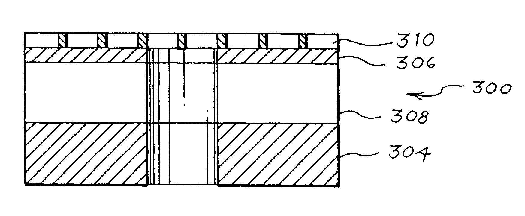
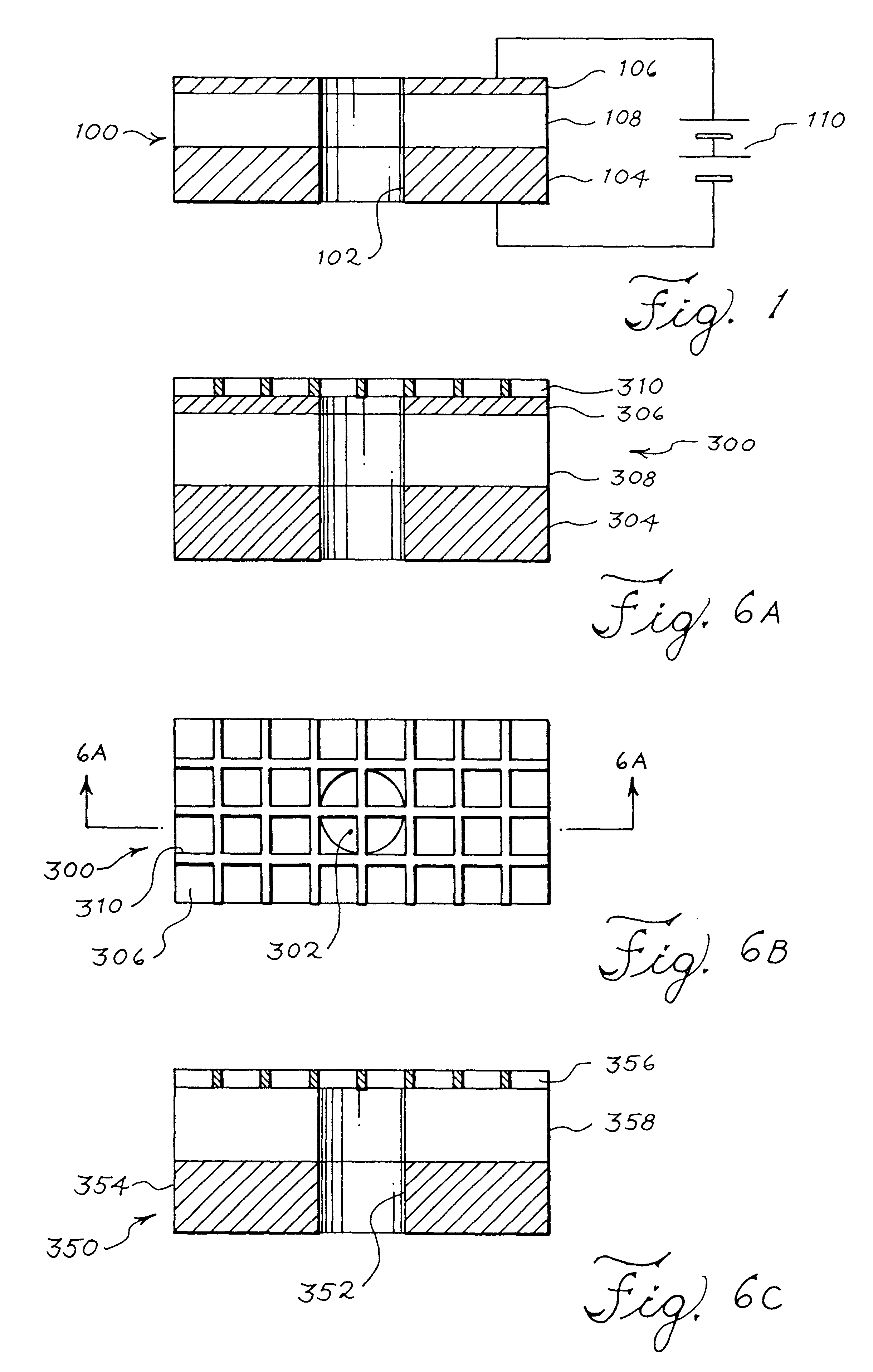
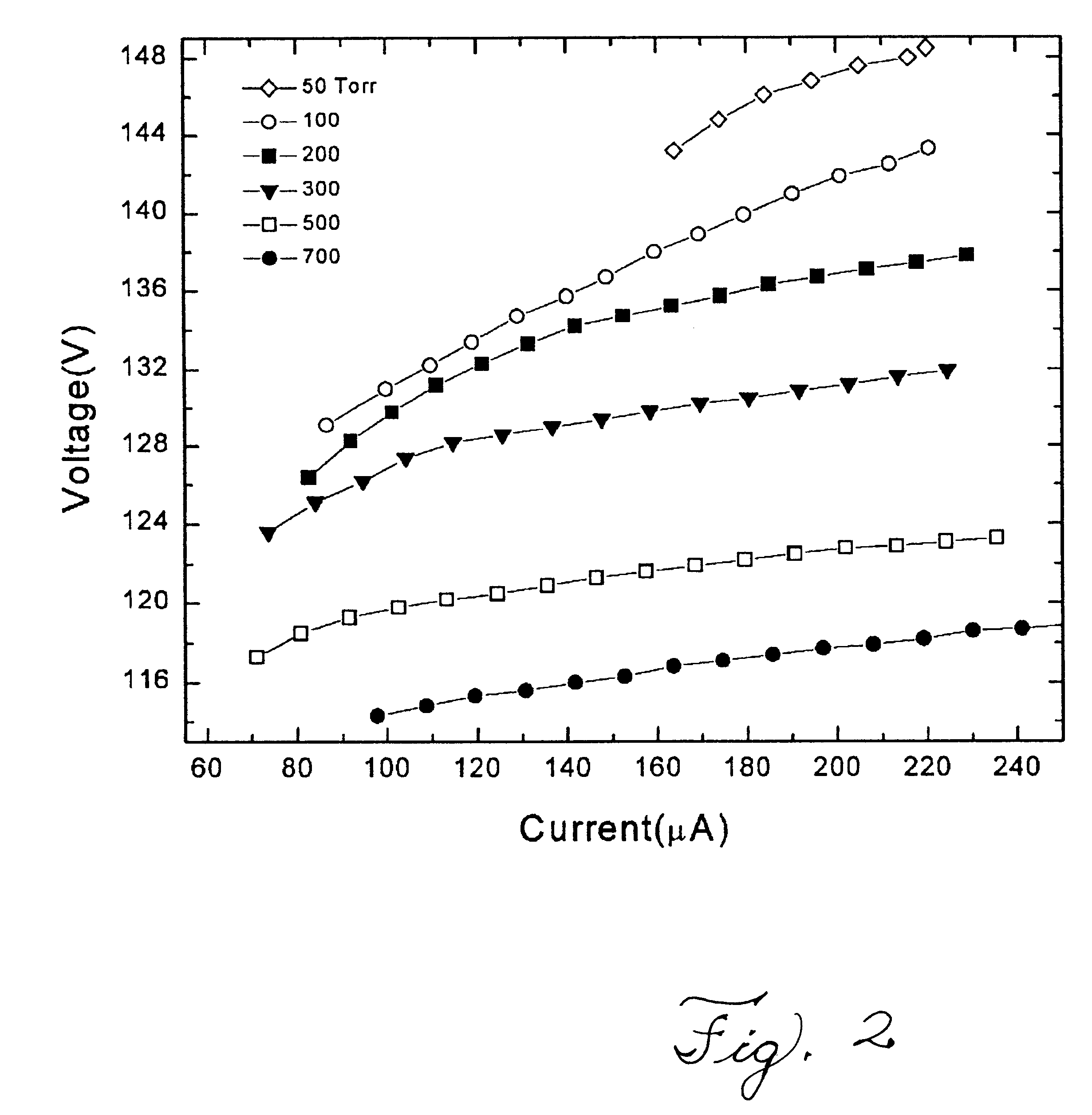
One example of such a microdischarge device 100 has a 25 .mu.m thick copper foil as the first electrode 106, a polyimide film 5-8 .mu.m thick as the insulator 108, and a 2000 .ANG. thick Ni film as a second electrode 104. FIG. 2 shows the voltage-current (V-I) characteristics for this Ni / polyimide / Cu microdischarge device. The polymer film for the insulator 108 was formed by spin coating a solution of 20 wt % of poly (trimetallic anhydride chloride-alt benzidine) in a 1-methyl-2-pyrolidinone / xylene solution on the copper foil. Residual solvent was evaporated by a hot plate and a vacuum drying process at >200.degree. C. The Ni second electrode 104 was next evaporated onto the polymer, giving a total device thickness of about 30 .mu.m. Microdischarge cavities 14 having a diameter of typically 150 .mu.m were then produced either by mechanically drilling or using a pulsed Ti:Al.sub.2 O.sub.3 laser to bore through the second electrode 104, insulator 108 and first electrode 106. Once fabr...


PUM


Abstract

A discharge device is described that contains an anode, a cathode, and an insulating layer disposed between the anode and the cathode. A cavity is extends entirely through at least one of the anode or cathode and penetrates the dielectric layer. At least one of the anode or cathode may include a screen or the dielectric layer may have a plurality of films with at least two different dielectric constants. The voltage differences between the anode and cathode in each of multiple devices electrically connected together may be limited.

Description

The present invention relates to microdischarge devices and, in particular, new structures for light emitting devices and low-cost methods of producing ultraviolet or visible light from thin sheets.It has long been known that electrical discharges are efficient sources of light and, today, gas discharge lamps (including fluorescent sources, and metal-halide, sodium, or mercury arc lamps) account for most of the world's light-generating capacity (several billion watts on a continuous basis). Most of these devices are, unfortunately, bulky and frequently have fragile quartz or glass envelopes and require expensive mounting fixtures. In addition to general lighting, discharges produce ultraviolet and visible light for other purposes such as germicidal applications (disinfecting surfaces and tissue), cleaning electronic and optical surfaces in manufacturing, and activating light-sensitive molecules for medical treatments and diagnostics.Although microdischarges were demonstrated by A. D...

Claims


Application Information

Patent Timeline
Patent Type & Authority Patents(United States)
IPC IPC(8): G09G3/04G09G3/10H01J25/00H01J61/06H01J63/00H01J63/04H01J25/50H01J1/00H01J9/00H01J17/04H01J1/62H01J1/02H01J9/24H01J61/62H01J65/04
CPCH01J1/025H01J9/02H01J61/09H01J61/305H01J61/62H01J65/046H01J9/00H01J25/50H01J63/04H01J17/49
Inventor EDEN, J. GARYPARK, SUNG-JINWAGNER, CLARK J.
Owner THE BOARD OF TRUSTEES OF THE UNIV OF ILLINOIS
Why Eureka
Try Eureka