Electron beam drawing mask blank, electron beam drawing mask, and method of manufacturing the same

Inactive Publication Date: 2004-11-02
HOYA CORP
View PDF12 Cites 81 Cited by
  • Summary
  • Abstract
  • Description
  • Claims
  • Application Information

AI Technical Summary

Benefits of technology

Therefore, an object of the present invention is to provide an electron beam drawing mask capable of solving the problems such as the beam contrast, the contro

Problems solved by technology

As the wiring pattern becomes the finer, the optical lithography technique or a general technique has found it the more difficult to form the pattern.
However, the various mask structures thus proposed have several problems from the standpoint of practice.
Because of the pattern of a high aspect ratio, on the other hand, there is a problem in the pattern sizing precision.
Because of the through holes, there is a problem on the mechanical strength of the mask.
Where the transfer pattern has the through holes, however, the ring-shaped (or donut-shaped) pattern or the like cannot be formed in a completely independent form.
According to this method, however, at least two times as many as masks are required, and the shot number of exposures are increased to invite a drastic elongation of the exposure time period.
This lowers the processing ability owned by the exposure system.
Moreover, a new problem occurs if the pattern region (or the thin film portion) is thinned to improve the working precision (or the pattern sizing precision).
Even if a polycrystalline diamond film having the largest elastic coefficient known at present is applied to the aperture body, however, it is difficult to reduce the deflection displacement to a practical level so long as the sectional area of the pattern supporting portion 4 shrinks.
In the SCALPEL mask (or the electron beam scattering mask), on the other hand, problems of the loss of the transmission electrons and the mask durability are caused by the electron beam scattering at the electron beam transmitting layer (or film) (as will be called the "pattern supporting layer (or film)" or the "membrane") by the mask structure.
Since the electron outgoing angle from the pattern supporting layer is within a predetermined range, however, the electrons having an outgoing an

Method used


Image

  • Electron beam drawing mask blank, electron beam drawing mask, and method of manufacturing the same
  • Electron beam drawing mask blank, electron beam drawing mask, and method of manufacturing the same
  • Electron beam drawing mask blank, electron beam drawing mask, and method of manufacturing the same

Examples


embodiment 1

(Embodiment 1)

Over a silicon substrate 11, as shown in FIG. 9A, an SiC layer 12 is formed to have a thickness of 0.03 micron as the pattern supporting layer (or film) by the CVD method. Over this SiC layer 12, an amorphous silicon (a-Si) layer 13 is formed (FIG. 9B) to have a thickness of 0.7 micron as the electron beam scattering layer by the CVD method. Subsequently, the back or under side of the substrate 11 is dry-etched to etch the Si thereby to form support members (or support pillars) 14 for supporting the pattern region (FIG. 9C).

Next, the upper face of the a-Si layer 13 is subjected to a lithography method (by the resist application, by the exposure, by the development and so on) to form a resist pattern 15 having a desired pattern shape (FIG. 9D).

Next, the a-Si layer 13 is etched (or trench-etched) at a high aspect ratio by the high-density plasma etching method (FIG. 9E). The etching selection ratio (SR) at this time is preferred to be as high as possible. In this embodim...

embodiment 2

(Embodiment 2)

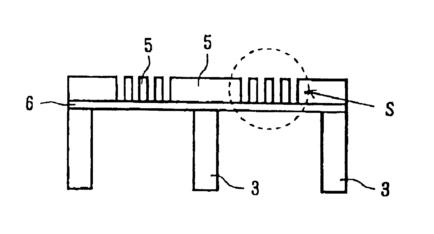
In a mask manufactured in Embodiment 2, the etching stopper layer 7 is sandwiched between the electron beam scattering layer 5 and the pattern supporting layer 6. This structure aims substantially at preventing the pattern supporting layer 6 from being etched by the etching stopper layer 7 at the time of etching the electron beam scattering layer 5, and is effective where the electron beam scattering layer 5 and the pattern supporting layer 6 have a small etching selection ratio. Another purpose for sandwiching the etching stopper layer 7 will be described in the following. Where a deflection is unpreferably caused in the pattern field portion due to the unbalance in the membrane stress between the electron beam scattering layer 5 and the pattern supporting layer 6, the membrane stress balance can be adjusted by adding the etching stopper layer 7. Thus, it is possible to give the etching stopper layer 7 the function to adjust the stress.

Here will be described an exampl...

embodiment 3

(Embodiment 3)

In Embodiment 3, here will be described the mask construction which can optimize the mask material while satisfying the mask characteristics of the present invention, and a method for manufacturing the mask.

In order to satisfy a structurally high strength and a high electron transmissivity in the mask, it is desired to reduce the film material density, to increase the material strength characteristics such as the Young's modulus, and to make the electron beam scattering body as thick as possible. In addition, the material is desired to make the pattern supporting layer as thin as possible, to have an excellent chemical resistance and an excellent irradiation resistance, and to have an excellent etchability from the view point of the pattern precision. Moreover, the material is desired not to be an insulating material while considering the charging.

Here will be enumerated the materials which satisfy those characteristics and the mask characteristics of the present inven...


PUM


Abstract

An electron beam drawing mask includes a pattern supporting film for transmitting an electron beam therethrough; an electron beam scattering body pattern formed over the pattern supporting film; and a support member for supporting the pattern supporting film and the electron beam scattering body pattern. The pattern supporting film has a film thickness of 0.005 to 0.2 micron, a film material density of 1.0 to 5.0 g/cm<3 >and an elastic modulus of 0.8x10<11 >Pa or higher. The electron beam scattering body pattern has a film thickness of 0.2 to 2 micron, a film material density of 1.0 to 5.0 g/cm<3>, and an elastic modulus of 0.8x10<11 >Pa or higher.

Description

The present invention relates to a transfer mask (or a reticle) to be used in a lithography technique for manufacturing a semiconductor device or the like by using a charged particle beam or an electron beam, a mask blank (or a mask forming substrate), and a method for manufacturing the mask.In order to form a wiring pattern or the like, there has been utilized the lithography technique. As the wiring pattern becomes the finer, the optical lithography technique or a general technique has found it the more difficult to form the pattern. For this difficulty, there has been investigated an exposure technique which uses a charged particle beam such as an electron beam or an ion beam or a short-wavelength beam such as an X-ray for the finer structure.Of these, the electron beam drawing technique has transferred from the point beam drawing method at the initial stage to the variable shape drawing method for drawing by changing the size and shape of a square beam. After this, from the stan...

Claims


Application Information

Patent Timeline
IPC IPC(8): G03F1/14G03F1/16G03F1/20H01L21/027
CPCG03F1/20H01L21/027
Inventor AMEMIYA, ISAO
Owner HOYA CORP
Why Eureka
Try Eureka