Curved fractional CMOS bandgap reference

a fractional cmos bandgap and fractional cmos technology, applied in the direction of electric variable regulation, process and machine control, instruments, etc., can solve the problems of length modulation, secondary effect of the transistor, etc., to speed up the response time, minimize the area, and precise voltage over the process

Inactive Publication Date: 2005-01-11
SILICON STORAGE TECHNOLOGY
View PDF2 Cites 30 Cited by
  • Summary
  • Abstract
  • Description
  • Claims
  • Application Information

AI Technical Summary

Benefits of technology

In one aspect, the present invention uses a bandgap including a mixed op amp operated in a continuous mode to provide precise voltage over process, temperature, power supply, and foundries. A HV level is provided at different level for different chip operation, and is settable by digital control bits, such as fuse bits at power up and/or at initialization of chip operations. A filter network filters out the ripple noise and charge transient. A mixed scheme helps to achieve the regulation, and may have both low voltage and high voltage devices as part of a circuit block to minimize area. The bandgap may also include certain elements to achieve more than one circuit function. A simulated resistor using HV PMOS in a certain configuration to achieve a precision divider ratio. A tracking capacitor divider tracks the simulated resistor ratio to speed up the response time.
A bandgap architecture is desirable to provide fractional bandgap voltage (<1.2V) and current that is suitable for nano-meter process technology. As technology progresses into the nano-meter regime, transistor performance is susceptible to secondary effect such as channel length modulation (CLM), breakdown (BV), gate or drain induced lowering (GIBL or DIBL), direct tunn...

Problems solved by technology

As technology progresses into the nano-meter regime, transistor performance is susceptible to secondary effect su...

Method used


Image

  • Curved fractional CMOS bandgap reference
  • Curved fractional CMOS bandgap reference
  • Curved fractional CMOS bandgap reference

Examples


Embodiment Construction

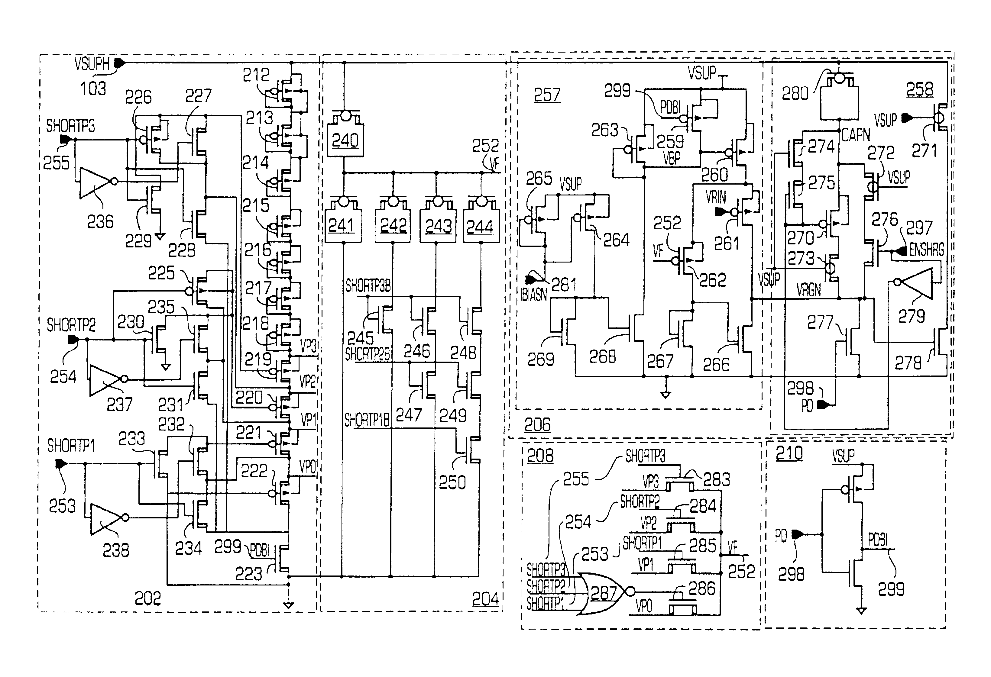
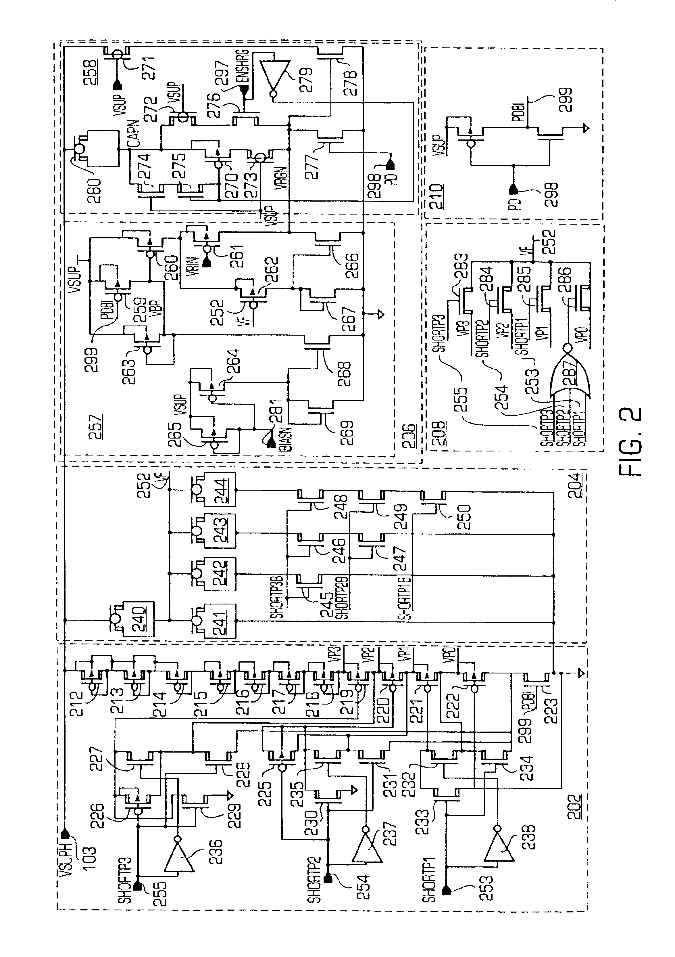
As used herein, a N-type NMOS enhancement transistor is an enhancement transistor having a gate threshold, for example in the range of approximately 0.3 to 1.0 volts. A P-type transistor is a PMOS enhancement transistor having a gate threshold approximately in the range of −0.3 to −1.0 volts. A NZ NMOS transistor is a native low voltage transistor having a gate threshold approximately in the range of −0.1 to 0.3 volts. An NH NMOS transistor is an enhancement high voltage transistor having a gate threshold approximately in the range of 0.3 to 1.0 volts. A PH PMOS transistor is an enhancement high voltage transistor having a gate threshold of approximately in the range −0.3 to −1.0 volts. An NX NMOS transistor is a native high voltage transistor having a gate threshold voltage approximately in the range −0.1 to 0.3 volts.

As used herein, the symbol VBEx is the voltage across the base-emitter of a transistor x, and a resistance Ry is the resistance of a resistor y.

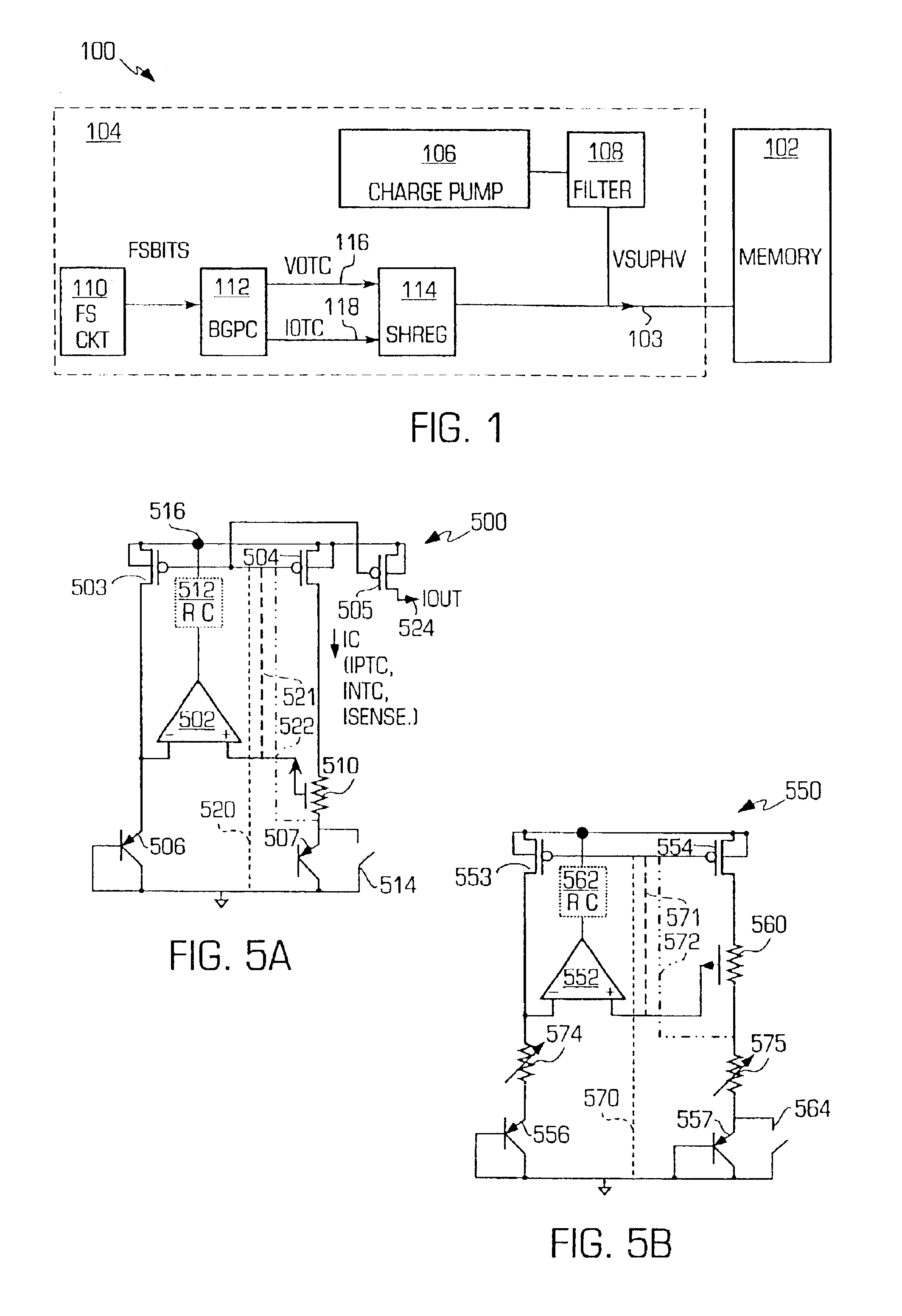
FIG. 1 is a block diag...


PUM


Abstract

A high shunt regulator provides precise voltage over process, temperature, power supply, and foundries. The HV level is settable by a digital control bits such as fuse bits. A filter network filters out the ripple noise and charge transient. A tracking capacitor divider network speeds up response time. A fractional band gap reference provides fractional bandgap voltage and current, and operates at low power supply and has superior power supply rejection. It is unsusceptible to substrate hot carrier effect. It exposes very little to drain induced barrier lowering effect. The bandgap core has better than conventional transient response and stability. One embodiment has adjustable level control. Complementary TC (temperature coefficient) trimming allows efficient realization of zero temperature coefficients of current and voltage. Higher order curvature correction of voltage and current is integrated. Replica bias for the control loop is presented. A Binary and Approximation Complementary TC search trimming is described. A zero TC fractional voltage less than the theoretical bandgap voltage (<<−1.2. Volt) is realizable. The bandgap core has a filtering mechanism to reject high frequency noise. A low power startup circuit powers up the band gap. The band gap also has variable impedance.

Description

BACKGROUNDThe invention relates to high voltage regulators, and more particularly high voltage regulators including a shunt regulator and / or a bandgap reference generator.A conventional mixed mode integrated circuit system frequently uses different voltage supplies. Analog signal processing, such as amplification, comparison, and pulse generation, may be performed at high voltage. A FLASH memory applies an erase signal and a program signal to memory cells. The erase signal and the program signal have voltage levels greater than a supply voltage. Also in multilevel volatile memories, the variation of the voltage level of the program signal falls in a smaller range for the multibit signals stored in the memory cells.A high voltage supply is typically used on-chip for non-volatile programming, erasing, and read operations. High voltage is generated typically from a charge pump utilizing capacitors. Regulation of the charge pumped high voltage provides precise voltage level for chip ope...

Claims


Application Information

Patent Timeline
IPC IPC(8): G05F3/08G05F3/30
CPCG05F3/30
Inventor TRAN, HIEU VAN
Owner SILICON STORAGE TECHNOLOGY
Why Eureka
Try Eureka