Dielectric layer for semiconductor device and method of manufacturing the same

Inactive Publication Date: 2005-01-18
SAMSUNG ELECTRONICS CO LTD
View PDF9 Cites 203 Cited by
  • Summary
  • Abstract
  • Description
  • Claims
  • Application Information

AI Technical Summary

Benefits of technology

Further, in accordance with the other aspect of the present invention, interface characteristics can be improved and the EOT can be maintained or reduced.
In addition, according to another aspect of the present invention

Problems solved by technology

However, because the silicon dioxide gate dielectrics has a low dielectric constant (k), e.g., 3.9, further scaling down of silicon dioxide gate dielectric thickness has become more and more difficult, especially due to gate-to-channel leakage current through thin silicon dioxide gate dielectrics.
Unfortunately, the use of high-k metal oxide materials presents several problems when using traditional substrate materials such as silicon.
This increases the equivalent oxide thickness, thereby degrading device performance.
Also, the high-k metal oxide layer such as a hafnium oxide (HfO2) layer or a zirconium oxide (ZrO2) layer has a relatively low crystallization temperature and is thermally unstable.
And the surface roughness of the metal oxide layer increases, deteriorat

Method used


Image

  • Dielectric layer for semiconductor device and method of manufacturing the same
  • Dielectric layer for semiconductor device and method of manufacturing the same
  • Dielectric layer for semiconductor device and method of manufacturing the same

Examples


Embodiment Construction

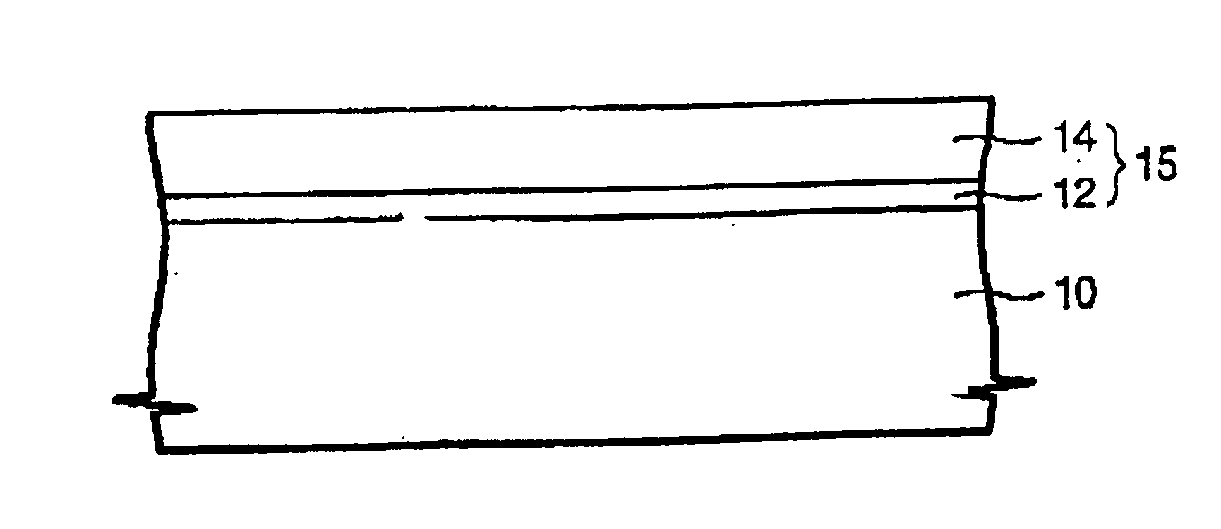
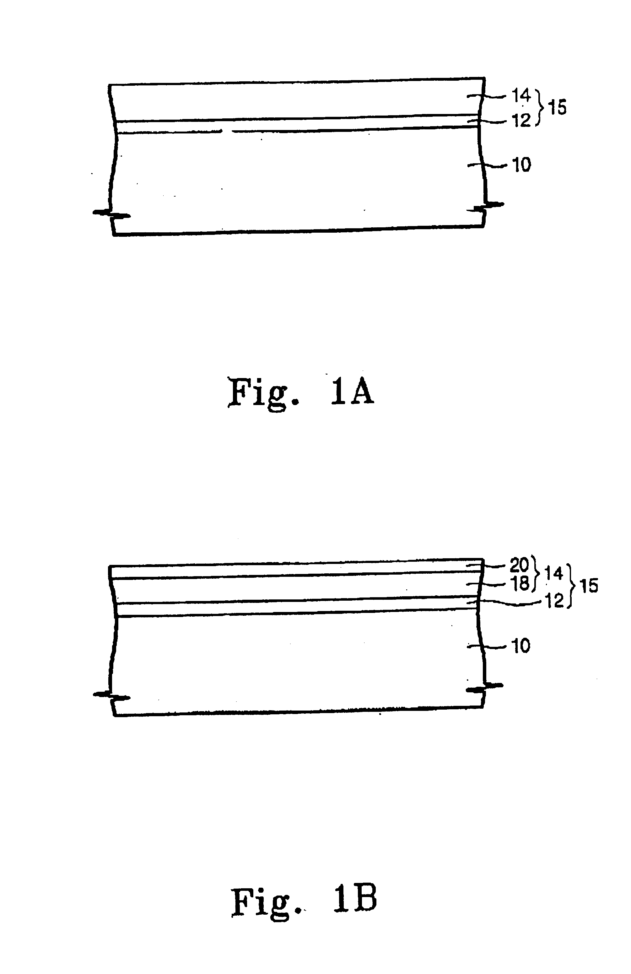
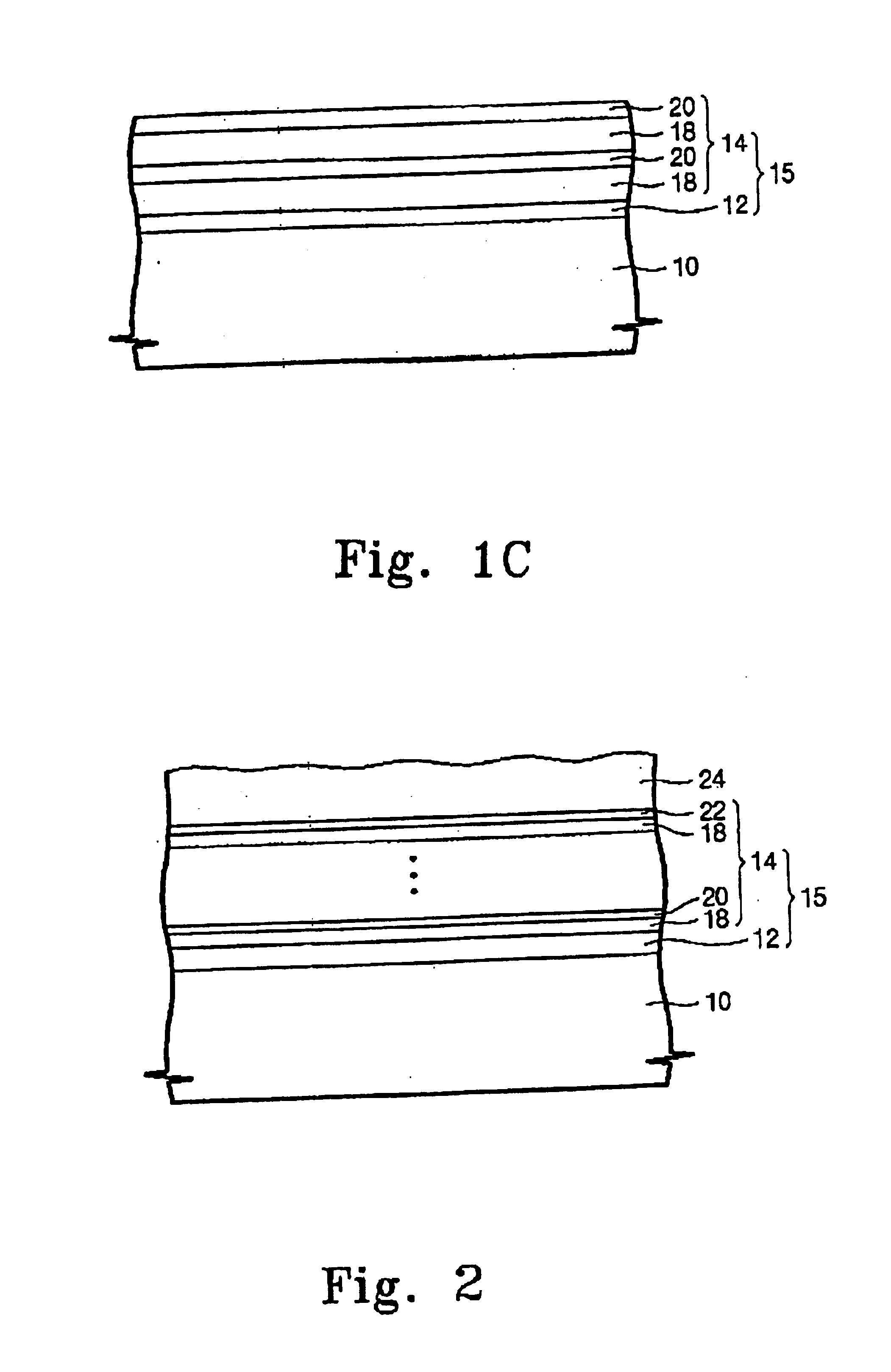
The present invention provides a noble dielectric layer structure and a method of manufacturing the same. In the following description, numerous specific details are set forth to provide a thorough understanding of the present invention. However, one having ordinary skill in the art should recognize that the invention can be practiced without these specific details. In some instances, well-known process steps, device structures, and techniques have not been shown in detail to avoid obscuring the present invention.

Although the invention is described in conjunction with gate dielectrics of a MOS transistor, the present invention is equally applicable to any dielectric for semiconductor devices, such as an inter-gate dielectric layer of non-volatile memory devices, or a dielectric layer of a storage capacitor, all of which are within the spirit and scope of the present invention.

The preferred embodiments of the present invention are best understood by referring to FIGS. 1-7 of the draw...


PUM

PropertyMeasurementUnit
Thicknessaaaaaaaaaa
Dielectric polarization enthalpyaaaaaaaaaa
Structureaaaaaaaaaa

Abstract

A multi-layer dielectric layer structure for a semiconductor device. The multi-layer dielectric layer structure comprises a silicate interface layer having a dielectric constant greater than that of silicon nitride and a high-k dielectric layer overlying the silicate interface layer. The high-k dielectric layer comprises one or more ordered pairs of first and second layers. With the present invention, the dielectric constant of the high-k dielectric layer can be optimized while improving interface characteristics. With a higher crystallization temperature realized by forming the multi-layer structure, each of whose layers is not more than the critical thickness, leakage current can be reduced, thereby improving device performance.

Description

BACKGROUND OF THE INVENTION1. Field of the InventionThis invention relates generally to the field of semiconductor devices, and more particularly, to a dielectric layer structure and a method of manufacturing the same.2. Description of the Related ArtWith each generation of metal oxide semiconductor (MOS) integrated circuit (IC), the device dimensions have been continuously scaled down to provide for high-density and high-performance devices. Particularly, the thickness of gate dielectrics is made as small as possible because the drive current in a MOS field effect transistor (FET) increases with decreasing gate dielectric thickness. Thus, it has become increasingly important to provide extremely thin, reliable, and low-defect gate dielectrics for improving device performance.For decades, a thermal oxide layer, e.g. silicon dioxide (SiO2), has been used as the gate dielectrics because the silicon dioxide thermal oxide layer is stable with the underlying silicon substrate and the fab...

Claims


Application Information

Patent Timeline
IPC IPC(8): H01L21/02H01L29/66H01L21/28H01L29/40H01L29/51H01L29/788H01L29/94H01L21/8247H01L21/31H01L21/316H01L21/822H01L21/8242H01L21/8246H01L27/04H01L27/105H01L27/108H01L27/115H01L29/78H01L29/792
CPCH01L21/28185H01L21/28194H01L21/28202H01L29/94H01L29/517H01L29/518H01L29/7881H01L29/513H01L28/56H01L21/31
Inventor LEE, JONGHOLEE, NAE-IN
Owner SAMSUNG ELECTRONICS CO LTD
Why Eureka
Try Eureka