

Temporary coatings for protection of microelectronic devices during packaging
a technology of microelectronic devices and coatings, applied in the field of microelectronics, can solve the problems of insufficient carrying capacity of conventional electronic packaging methods, although expensive, and the loss of probed “good” mems in significant quantities, and achieve the effects of reducing the risk of release of delicate mems elements, and reducing the number of conductive coatings
- Summary
- Abstract
- Description
- Claims
- Application Information
AI Technical Summary
Problems solved by technology
Method used
Image

Examples
Embodiment Construction
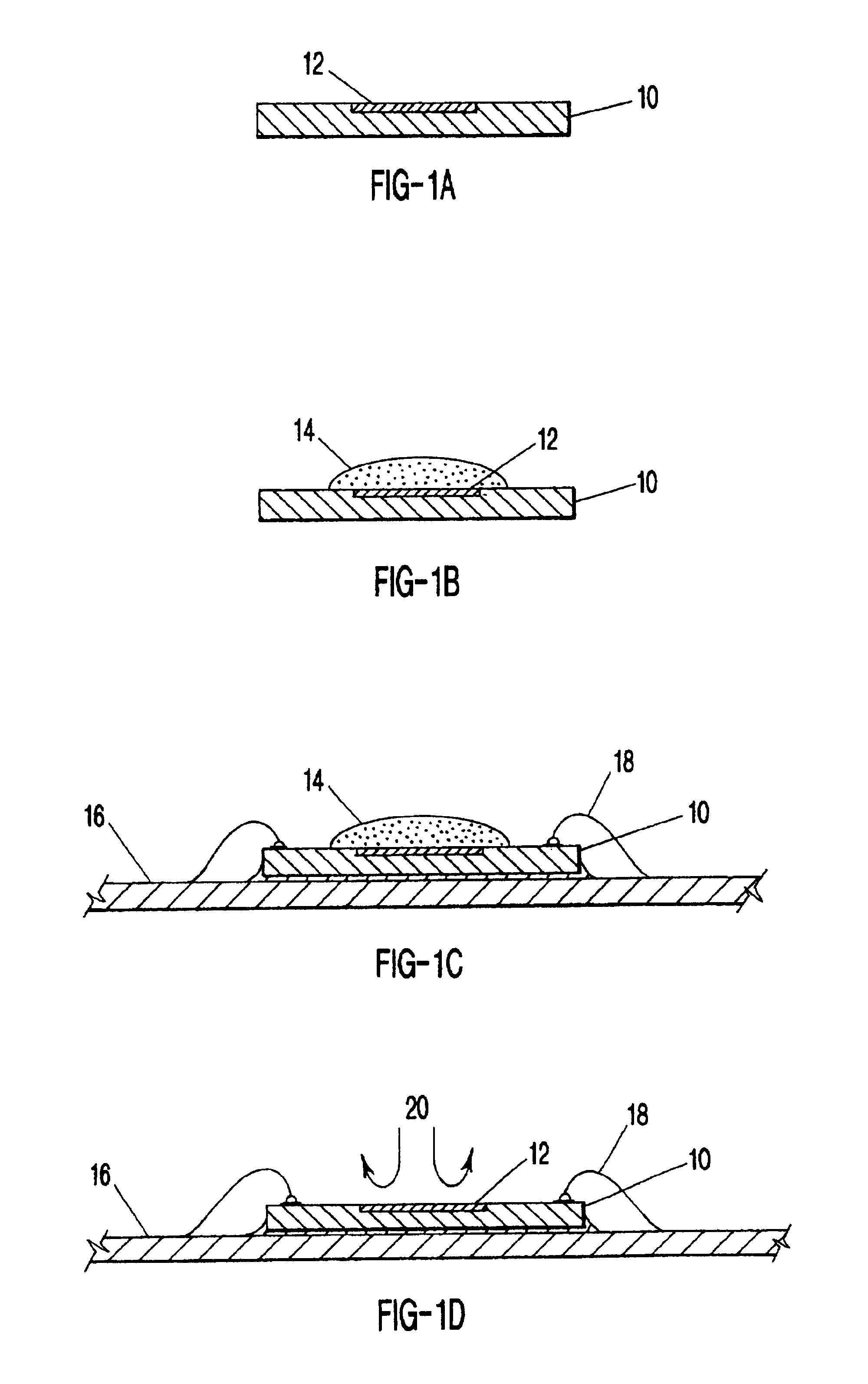
The present invention relates to a method of protecting a microelectronic device during device packaging, comprising, in the order presented: providing a microelectronic device having a sensitive area; applying a water-insoluble, protective coating to the sensitive area; performing at least one packaging step; and then substantially removing the protective coating from the sensitive area.
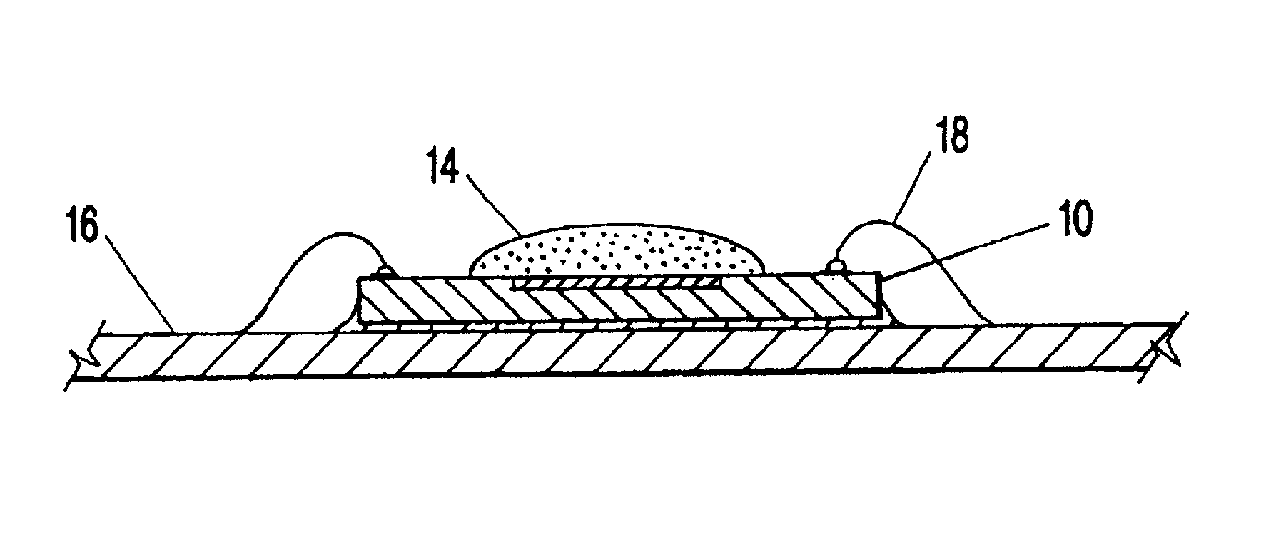
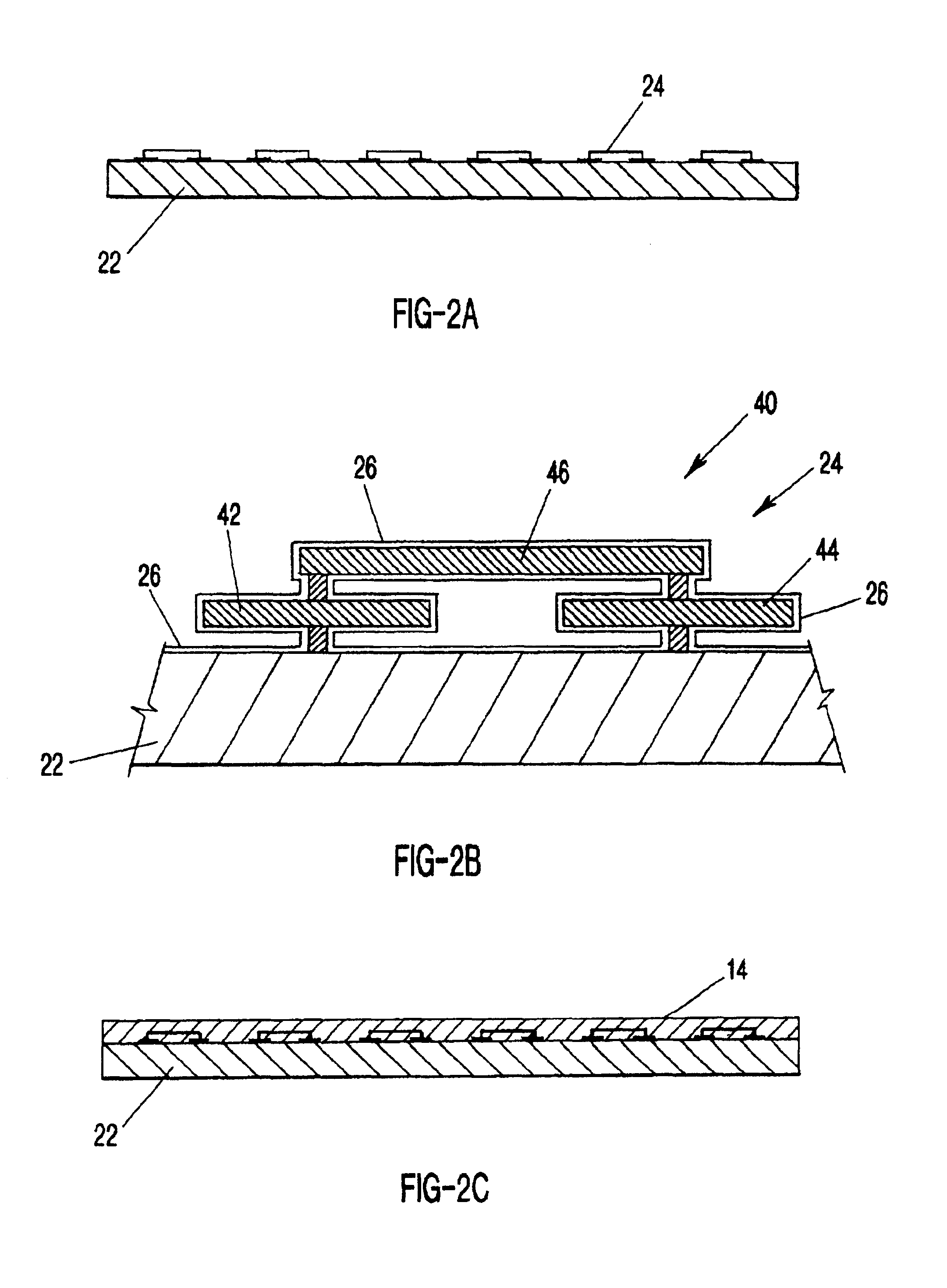
FIG. 1A shows a schematic cross-section view of a first example, according to the present invention, of a microelectronic device 10 with a sensitive area 12. Examples of microelectronic device 10 can include an airbag accelerometer, a microengine, an optical switch, a gyroscopic device, a microsensor, and a microactuator. Microelectronic device 10 can include microelectromechanical systems (MEMS) that have MEMS elements (e.g. gears, hinges, levers, slides, and mirrors). These freestanding MEMS elements must be free to move, rotate, etc during MEMS operation. Microelectronic device 10 can also includ...
PUM
| Property | Measurement | Unit |
|---|---|---|
| thickness | aaaaa | aaaaa |
| thick | aaaaa | aaaaa |
| electrically interconnected | aaaaa | aaaaa |
Abstract
Description
Claims
Application Information