Semiconductor laser device, semiconductor laser module, and optical fiber amplifier using the device or module

a semiconductor laser and laser module technology, applied in the direction of semiconductor lasers, optical resonator shape and construction, semiconductor laser arrangements, etc., can solve the problems of difficult to obtain constant amplification gain in edfa, and complicated process of fabrication of optical fiber amplifiers, so as to achieve stable amplification of signal lights and constant absorption coefficient

Inactive Publication Date: 2005-01-18
FURUKAWA ELECTRIC CO LTD
View PDF8 Cites 16 Cited by
  • Summary
  • Abstract
  • Description
  • Claims
  • Application Information

AI Technical Summary

Benefits of technology

It is an object of the present invention is to provide a semiconductor laser device, a semiconductor laser module and an optical fiber amplifier in which the amplification fiber maintains the constant absorption coefficient in spite of variation in temperature without requiring a temperature control module and obtains a stable amplification of signal lights in EDFA.
It is also an object of the present invention to realize a semiconductor laser device and a semiconductor laser module which are suitable for an excitation light source for the Raman amplifier or the like, are compact and easily produced, having a small degree of polarization and capable of suppressing stimulated Brillouin scattering, and to provide an optical fiber amplifier which enables stable and high-gain amplification that does not depend on the direction of polarization of the signal light.

Problems solved by technology

However, there are some requirements in the selection of excitation light source for the currently available optical fiber amplifiers requires caution.
Hence it is very difficult to obtain a constant amplification gain independent on the temperature change of exciting laser in the EDFA.
This indicates that it is not possible to obtain a constant amplification gain in EDFA independent of the oscillating wavelength change due to the temperature change of active layer of the laser.
When the laser beams to be polarization-combined are emitted from different semiconductor elements, the process of fabrication of the optical fiber amplifier become complicated and the optical fiber amplifier becomes bulky.
The semiconductor module used in the prior art 1 has a complex structure and function and besides is not cost-effective.
Particularly, since the thermo-electronic cooler consume electricity to cool the semiconductor laser device, total power consumption of semiconductor laser module also goes up.
Complex structure translates to uneconomical production time and cost.
Also, there is a high probability of breakdown.
An optical fiber amplifier is expected have a long and trouble-free service life.
There are problems with the prior art 2 as well.
The result is inability to maintain a constant gain.
On the other hand, when a semiconductor laser element having a structure of plural stripes, particularly a structure of two stripes (W-stripe structure) is used in the Raman amplifier, a new problem arises.
In other words, since a stable amplification gain cannot be obtained, the semiconductor laser element having the W-stripe structure is not suitable has a problem for use as an excitation light source of the Raman amplifier.
However, since the distance between the stripes in the semiconductor laser element is only within about a few hundred μm, it is neither easy nor realistic to carry out cleavage separately.
However, the production process of the Raman amplifier having the structure shown in FIG. 80 is complex and further it is difficult to miniaturize the entire device.
However, when its peak value is high, stimulated Brillouin scattering occurs, and this results in noise.

Method used


Image

  • Semiconductor laser device, semiconductor laser module, and optical fiber amplifier using the device or module
  • Semiconductor laser device, semiconductor laser module, and optical fiber amplifier using the device or module
  • Semiconductor laser device, semiconductor laser module, and optical fiber amplifier using the device or module

Examples


eighth embodiment

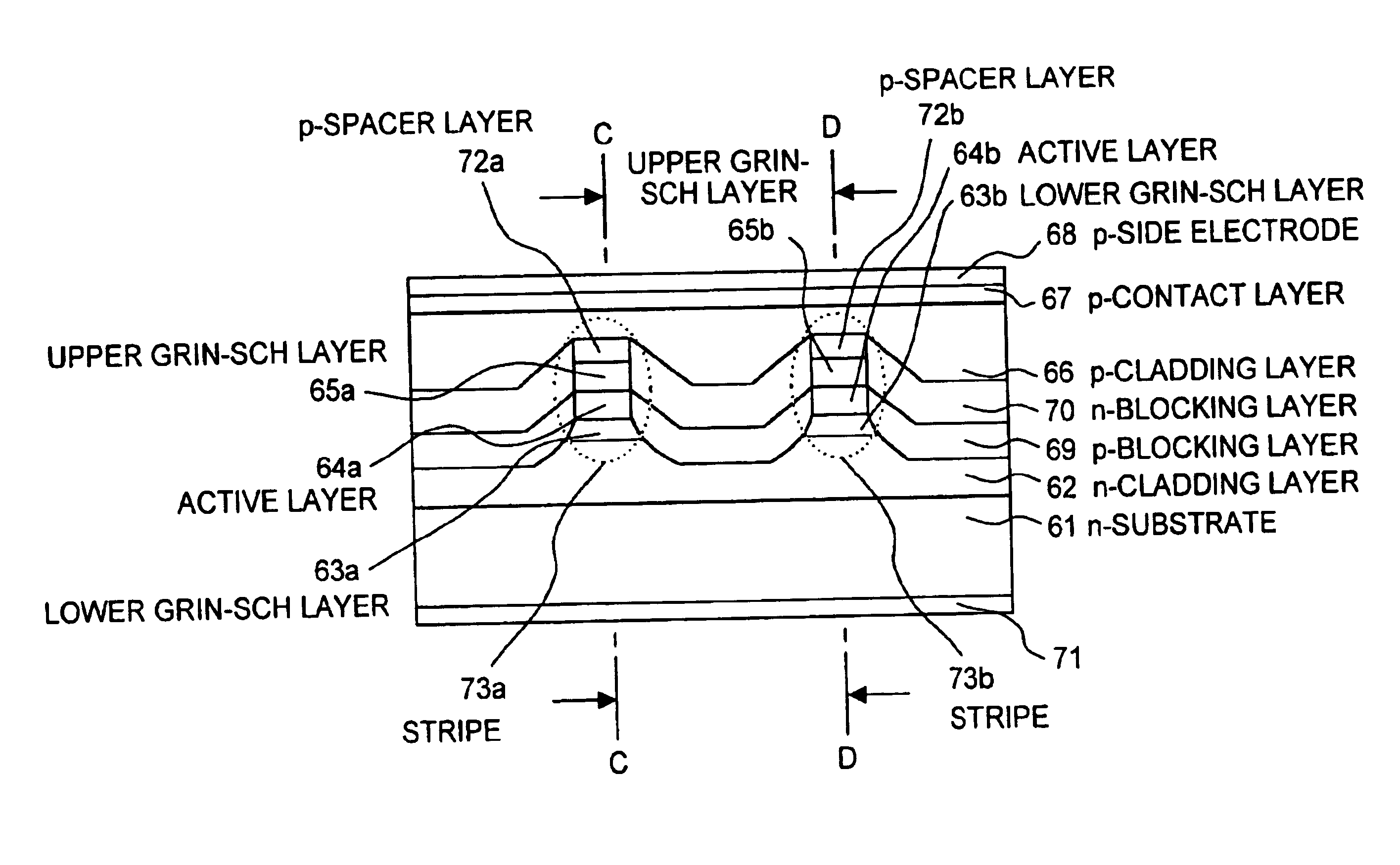
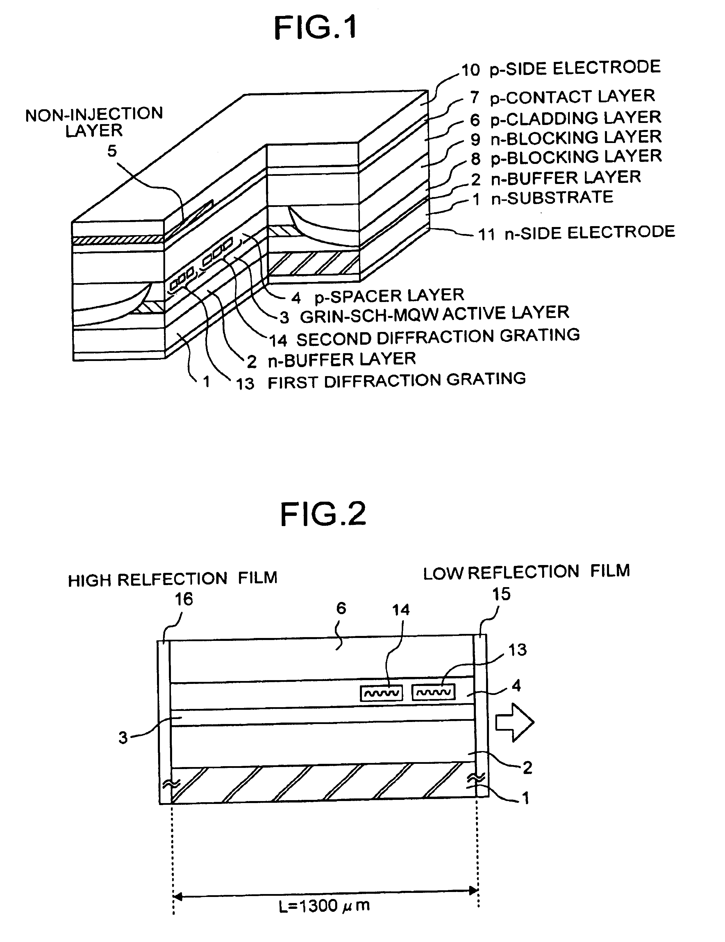
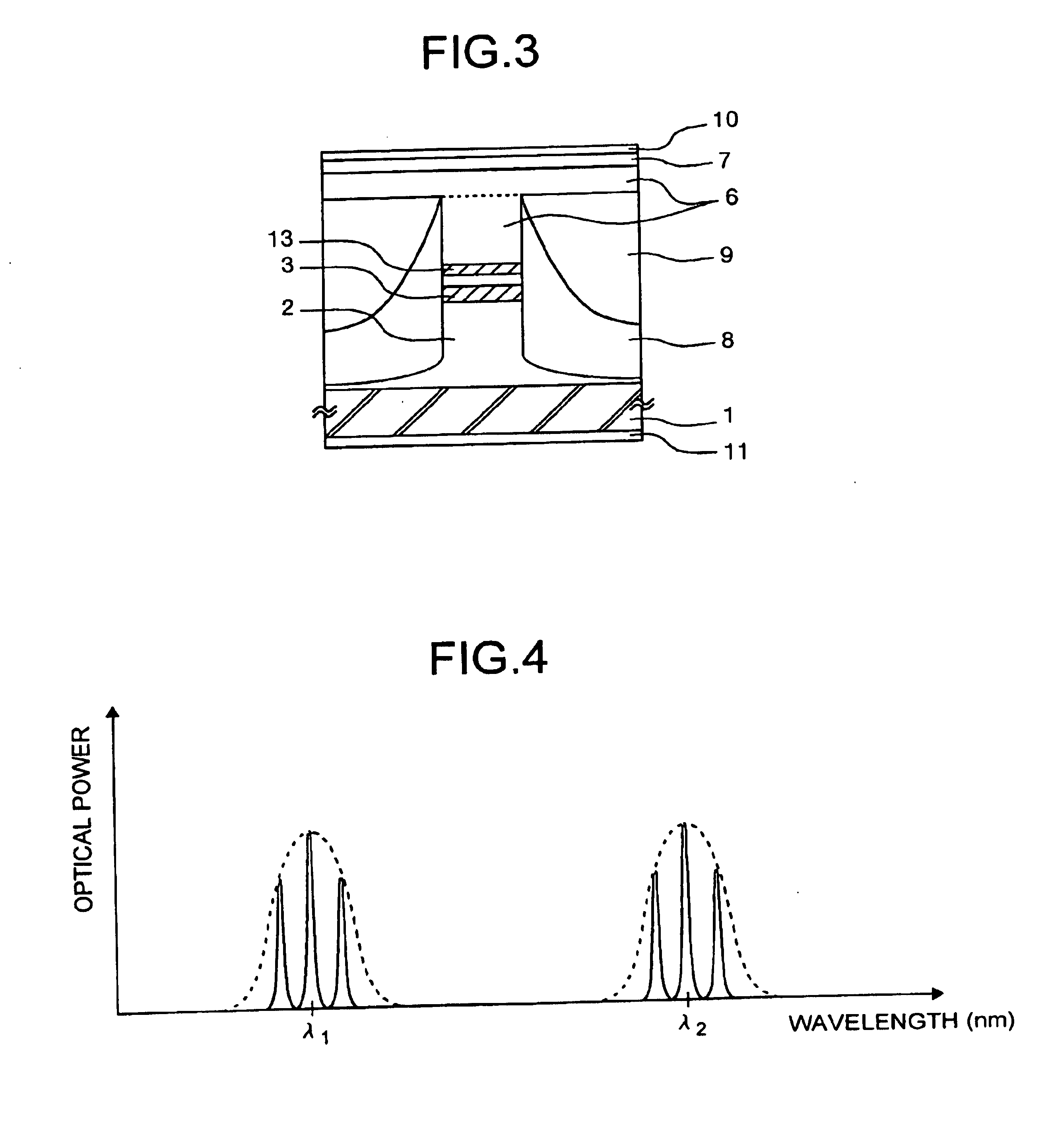
the present invention will be explained. FIG. 35 is a longitudinal sectional view in a longitudinal direction of a semiconductor laser device according to the eighth embodiment of the present invention. FIG. 36 is a sectional view of the semiconductor laser device shown in FIG. 35 taken along the line A—A. A sectional view along the line B—B shall be the same as the sectional view taken along the line A—A and so it is not shown.

The semiconductor laser device according to the eighth embodiment is constituted so that, as shown in FIG. 35, an n-InP cladding layer 1002 is laminated on an n-InP substrate 1001. Moreover, on the line A—A shown in FIG. 35, a lower GRIN-SCH layer 1003a, an active layer 1004a, and an upper GRIN-SCH layer 1005a are laminated in a mesa shape. These layers form a stripe 1015. Similarly, on the line B—B, a lower GRIN-SCH layer 1003b, an active layer 1004b and an upper GRIN-SCH layer 1005b are laminated in a mesa shape. These layers form another stripe 1016. The s...

twelfth embodiment

the present invention will be explained next. A semiconductor laser module according to the twelfth embodiment uses the semiconductor laser device of the eighth embodiment.

FIG. 55 is sectional view that shows a structure of the semiconductor laser module of the twelfth embodiment. FIG. 56 is a frame format of the structure of a semiconductor laser module according to the twelfth embodiment of the present invention.

As shown in FIG. 55, the semiconductor laser module of the twelfth embodiment has a package 1051 inside of which is tightly sealed, a semiconductor laser device 1052 which is provided in the package 1051 and emits a laser beam, a photodiode 1053, a first lens 1054, a prism 1055, a half-wave plate (polarization rotating device) 1056, a polarization beam combiner (PBC) 1057 and an optical fiber 1058.

As shown in FIG. 56, the semiconductor laser device 1052 has stripes 1015 and 1016 that are formed in parallel on the same plane in the longitudinal direction and are separated. ...

thirteenth embodiment

the present invention will be explained. In the thirteenth embodiment, noise is reduced by applying reverse modulation frequency signal to each stripe of a semiconductor laser device according to ninth or eleventh embodiment in which the stripes are electrically separated. Further, laser beam emitted from each stripe is polarized multiplexed in the semiconductor laser module according to twelfth embodiment. By depolarizing the polarization multiplexed laser beam, the intensity modulation of each plane of polarization is averaged out. In addition, the stimulated Brillouin scattering is also reduced.

The depolarizer used in the thirteenth embodiment of the present invention will be explained. FIG. 59 shows a structure of the semiconductor laser device including the depolarizer used in the thirteenth embodiment of the present invention. In this semiconductor laser, a semiconductor laser element 1081 and a polarization-maintaining optical fiber 1082 are fused and connected by fuse 1083. ...


PUM


Abstract

An n-side electrode, an n-substrate, an n-buffer layer, a GRIN-SCH-MQW active layer, a p-spacer, a p-cladding layer, a p-contact layer, and a p-side electrode are laminated one on top another in that order. Above the n-buffer layer, the GRIN-SCH-MQW layer and the p-spacer layer occupy a narrower area than the n-substrate in a direction that is at right angles to the laser emission direction, wherein the remaining area is occupied by a p-blocking layer and an n-blocking layer. Within the p-spacer layer are embedded a first diffraction grating and a second diffraction grating. Between the first and the second diffraction grating and the p-side electrode is provided a current non-injection area.

Description

BACKGROUND OF THE INVENTION1) Field of the InventionThe present invention relates, in general, to amplification of signal light in optical networking and in particular, to a semiconductor laser device that does not require a temperature control module. Particularly, the present invention relates to an erbium doped optical fiber amplifier (EDFA) that produces a stable amplification gain of signal light. Further, the invention relates to a semiconductor laser device that has two stripe structures, a semiconductor laser module and an optical fiber amplifier that is compact and easy to manufacture, and achieves high output power while reducing stimulated Brillouin scattering in Raman amplifier and the degree of polarization of the laser beam emitted from the semiconductor laser device.2) Description of the Related ArtWith the recent advancements in the field of optical networking which has internet technology at its core, an optical fiber amplifier embedding between the each span of the...

Claims


Application Information

Patent Timeline
Patent Type & Authority Patents(United States)
IPC IPC(8): H01S5/00H01S5/12H01S5/40H01S3/06H01S3/067H01S3/094H01S3/0941H01S3/30H01S5/022H01S5/0625
CPCH01S5/12H01S3/06729H01S5/4031H01S3/0941H01S3/09415H01S3/302H01S5/005H01S5/02248H01S5/02284H01S5/06256H01S5/1096H01S5/1203H01S5/1215H01S5/4012H01S3/094003H01S5/02325H01S5/02251
Inventor WAKISAKA, TSUYOSHITSUKIJI, NAOKIYOSHIDA, JUNJIKIMURA, TOSHIONAMIKI, SHU
Owner FURUKAWA ELECTRIC CO LTD
Why Eureka
Try Eureka