Method and apparatus for electroless deposition with temperature-controlled chuck

a technology of electroless deposition and temperature control, applied in the direction of spraying apparatus, liquid/solution decomposition chemical coating, coating, etc., can solve the problems of increasing maintenance requirements, non-uniform deposition of plated metallic materials, and increasing the complexity of electroplating equipment, so as to prevent thermal decomposition of solution, reduce the formation of gas bubbles, and prevent the accumulation of bubbles on the surface of the substrate.

Inactive Publication Date: 2005-01-25
LAM RES CORP
View PDF13 Cites 13 Cited by
  • Summary
  • Abstract
  • Description
  • Claims
  • Application Information

AI Technical Summary

Benefits of technology

The method of the invention consists in that electroless deposition of a coating material, which may be a metal, semiconductor, or dielectric, is carried out at a relatively low temperature of the working solution compensated by an increased temperature on the substrate which is controlled by a heater built into the substrate chuck. A decrease in the temperature of the working solution prevents thermal decomposition of the solution and reduces formation of gas bubbles, normally generated at increased temperatures. Accumulation of bubbles on the surface of the substrate is further prevented due to upwardly-facing orientation of the treated surface of the substrate. The remaining units of the apparatus, i.e., a closable chamber with inlet ports for the supply of various process liquids and a port for the supply of a gas under pressure, reservoirs and tanks for processing liquids and gases, a solution heater and a control system for controlling temperature and pressure in the chamber, etc. are the same as in the apparatus disclosed in the aforementioned earlier patent application of the same applicant.

Problems solved by technology

Disadvantages associated with electroplating are technical problems in connection with designing of reactors used in the electroplating of semiconductor wafers.
This non-uniform distribution of current across the wafer, in turn, causes non-uniform deposition of the plated metallic material.
But such thieving techniques add to the complexity of electroplating equipment, and increase maintenance requirements.
The specific metal to be electroplated can also complicate the electroplating process.
As a consequence, use of the typical plurality of electrical wafer contacts (for example, eight discrete contacts) may not provide adequate uniformity of the plated metal layer on the wafer.
Beyond the problems discussed above, there are also other problems associated with electroplating reactors.
Still further, existing electroplating reactors are often difficult to maintain and / or reconfigure for different electroplating processes.
One drawback associated with copper deposition by electroplating is the fact that for very small features on microelectronic workpieces (sub 0.1 micron features), copper deposition by electroplating can lack conformity with the side walls of high aspect ratio vias and trenches, and can produce voids in the formed interconnects and plugs (vias).
This is often due to the non-conformity of the copper seed layer deposited by PVD or CVD.
As a result, the seed layer may not be thick enough to carry the current to the bottom of high aspect ratio features.
It should be noted that a common problem in using bathes, which is especially true for the electroless deposition process, is that foreign particles or contaminants will be deposited on the substrate surface of the wafer when transferring the wafers from one bath to another bath.
Another common problem is the exposure of the substrate surface of the wafer to air during the transfer (from bath to bath) can cause the non-wetting of deep and narrow trenches in the surface or small (contact) holes in the surface because of electrolyte evaporation.
And yet another common problem is that exposure to air may cause oxidation of the catalytic surface that will result in poor catalytic activity and poor quality metal deposits.
This problem becomes especially troublesome when using materials such as copper that easily oxidize in air.
However, the processing chamber is an open-type chamber and therefore does not allow pressure-controlled deposition processes.
In addition, the open-type chamber does not provide adequate protection of the process against contamination of the solution.
Furthermore, for the metal interconnects on the surface of the wafer one of the major requirements is low resistivity.
However, due to the presence of various additives in the interface between the PVD Cu seeds and ECD Cu, resistivity is disproportionally increased as compared to much thinner electroless-deposited Cu layers.
However, it is understood that electroless deposition at high temperatures leads to significant non-unifornities in the deposited layers.
This, in turn, increases the cost of the equi merit and maintenance.
Such equipment requires a large production space and dictates the use of large volumes of the solutions.
Furthermore, an additional space is needed for the preparation, storage, and post-use treatment of the solutions.
This, in turn, creates environmental problems.
Another common drawback of existing electroless deposition apparatuses is low speed of deposition, which in general depends on the type of the deposited material and even in the best case does not exceed 100 nm / min, but normally is much lower.
However, although an elevated temperature of the working solution leads to essential increases in the productivity of the deposition process, the process requires constant replacement of the working solution since high temperature causes rapid thermal decomposition of the solution.
Constant replacement of the solution should be carried out with high flow rates, and this, in turn, increases the cost of the production.
The main disadvantage of the apparatus of the aforementioned International Application is that the substrate is oriented with the treated surface facing down.
It is known that in a static condition of the solution or in processes with low-velocity flows of the solution, the aforementioned orientation of the substrate leads to accumulation of gas bubbles on the treated surface.
Furthermore, differential velocities of the flow on the substrate surface may lead to non-uniform temperature distribution.
In other words, the apparatus of the International Application does not provide uniformity of electroless deposition.
Such a complicated system makes the apparatus and products more expensive, while the process becomes difficult to control.

Method used


Image

  • Method and apparatus for electroless deposition with temperature-controlled chuck
  • Method and apparatus for electroless deposition with temperature-controlled chuck
  • Method and apparatus for electroless deposition with temperature-controlled chuck

Examples


Embodiment Construction

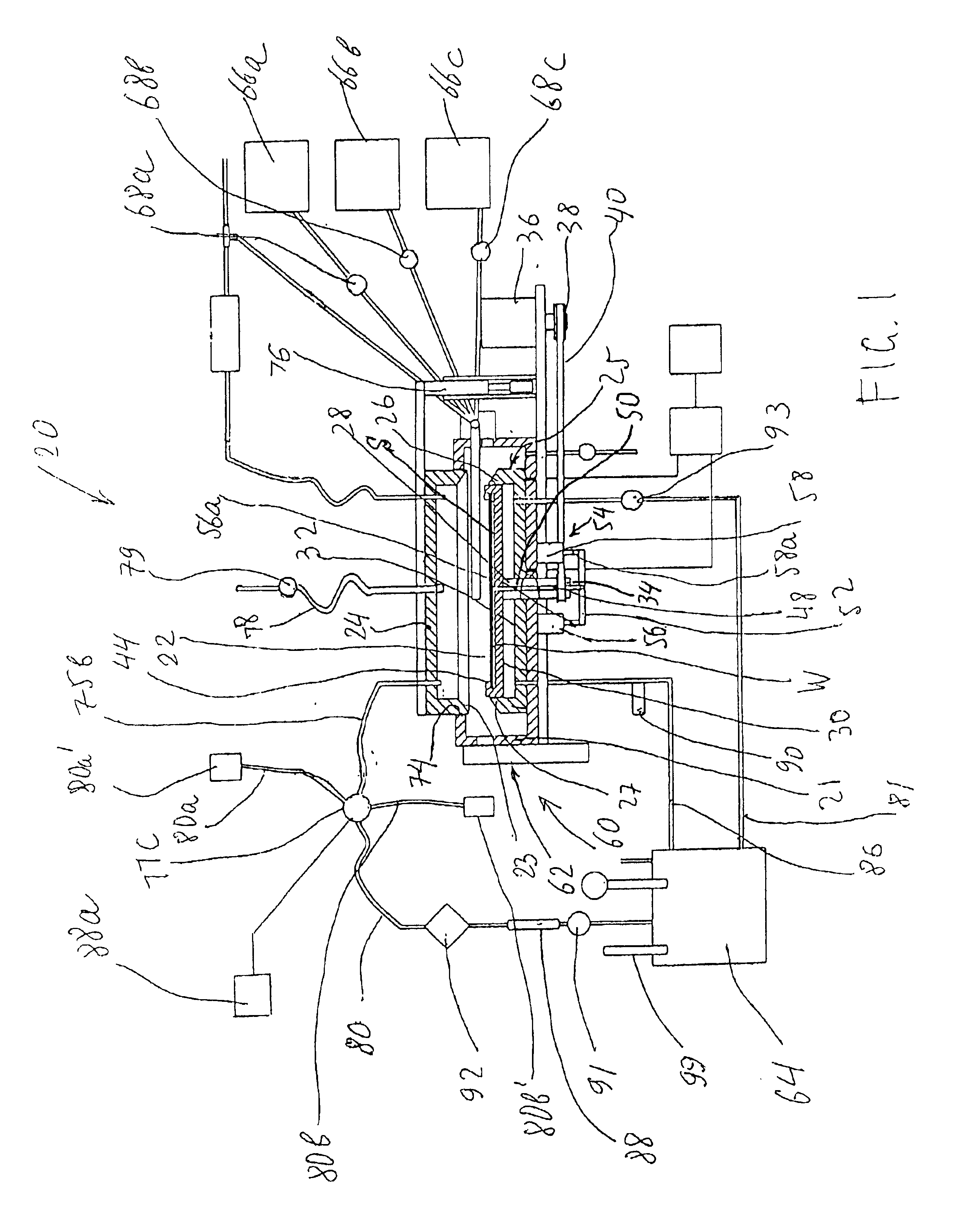
The electroless-plating apparatus of the invention, which is schematically shown in FIG. 1 and is designated as a whole by reference numeral 20, has a housing 21 that contains an electroless-plating chamber 22 (hereinafter referred to as “chamber 22”) that can be hermetically closed with a cover 24 located above the chamber 22. In a closed state, the chamber 22 may withstand increased pressures and is provided with appropriate seals (not shown) between the connected parts, such as the cover, chamber, ports, feedthrough devices, fittings, etc. More specifically, the pressure that can be developed inside the chamber 22 may reach 2 atmospheres above the atmospheric pressure or be reduced below the atmospheric pressure, e.g., down to 0.1 atmospheres.

The chamber 22 is either made of or has the inner surface coated with a chemically stable material that can withstand the action of aggressive solutions used in the operation process of the apparatus 20 under high temperatures and under high...


PUM

PropertyMeasurementUnit
temperatureaaaaaaaaaa

Abstract

The method for electroless deposition of a coating material, which may be a metal, semiconductor, or dielectric, that is carried out at a relatively low temperature of the working solution compensated by an increased temperature on the substrate which is controlled by a heater built into the substrate chuck. A decrease in the temperature of the working solution prevents thermal decomposition of the solution and reduces formation of gas bubbles, normally generated at increased temperatures. Accumulation of bubbles on the surface of the substrate is further prevented due to upwardly-facing orientation of the treated surface of the substrate. The substrate holder is equipped with a substrate heater and a substrate cooler, that can be used alternatingly for quick heating or cooling of the substrate surface.

Description

FIELD OF THE INVENTIONThe present invention relates to the field of semiconductor production, in particular, to an apparatus and method for electroless deposition of materials on semiconductor substrates. More specifically, the invention relates to electroless deposition with the use of a temperature-controlled chuck, which holds a substrate onto which a deposition is applied from a solution in the form of a thin metal film.BACKGROUND OF THE INVENTIONManufacturing of semiconductor devices, in particular integrated circuits having multiple-layered structures with various metal and non-metal layers laminated on a semiconductor substrate, typically involves an application of several metal layers onto a substrate or onto other previously deposited layers. These layers may have a complicated planar topology since these layers may constitute thousands of individual devices, which in combination form an integrated circuit or so-called “chip”. Modem chips may have metal or dielectric layers...

Claims


Application Information

Patent Timeline
Patent Type & Authority Patents(United States)
IPC IPC(8): C23C18/16H01L21/00
CPCC23C18/1619C23C18/1676H01L21/67109C23C18/168C23C18/1682C23C18/1678H01L21/20H01L21/68
Inventor IVANOV, IGOR C.ZHANG, JONATHAN WELGUNKOLICS, ARTUR
Owner LAM RES CORP
Why Eureka
Try Eureka