Thin film transistor

a technology of thin film semiconductors and transistors, applied in the direction of semiconductor devices, electrical equipment, transistors, etc., can solve the problems of not being profitable, not low concentration of elements contaminated in the insulating substrate usable for a thin film semiconductor device, and difficulty in sending out strange elements to the outside in case of contaminating, etc., to achieve the effect of convenient

Inactive Publication Date: 2005-02-01
SEMICON ENERGY LAB CO LTD
View PDF41 Cites 129 Cited by
  • Summary
  • Abstract
  • Description
  • Claims
  • Application Information

AI Technical Summary

Benefits of technology

FIG. 4 shows one preferred example of the present invention, and the present invention is not limited to the above process. In the example of FIG. 4, a silicon nitride film, a gate electrode, and a source or a drain region do not adjoin, like the example of FIG. 3. That is, the case of FIG. 4 is different

Problems solved by technology

Also in case of the monolithic integrated circuit, such alkaline ion as sodium and potassium, or such transition metal ion as iron, copper, and nickel poses a serious contamination problem, and much attention has been paid to stop the intrusion of these ions.
However, in general, the concentration of elements contaminated in an insulating substrate usable for a thin film semiconductor device is not low.
But it is not actual from a profitable point of view.
But it is dif

Method used


Image

  • Thin film transistor
  • Thin film transistor
  • Thin film transistor

Examples


example 1

EXAMPLE 1

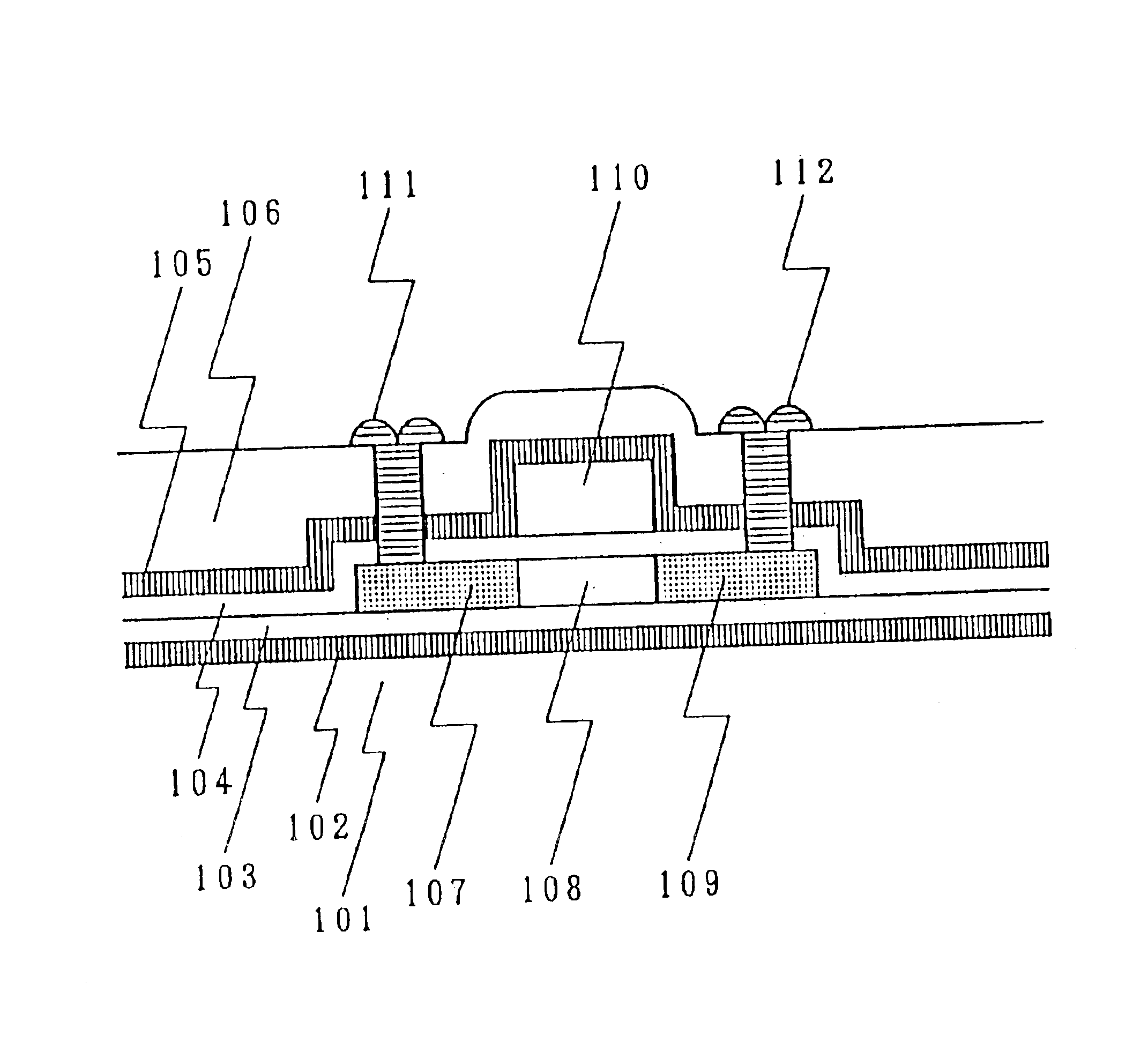
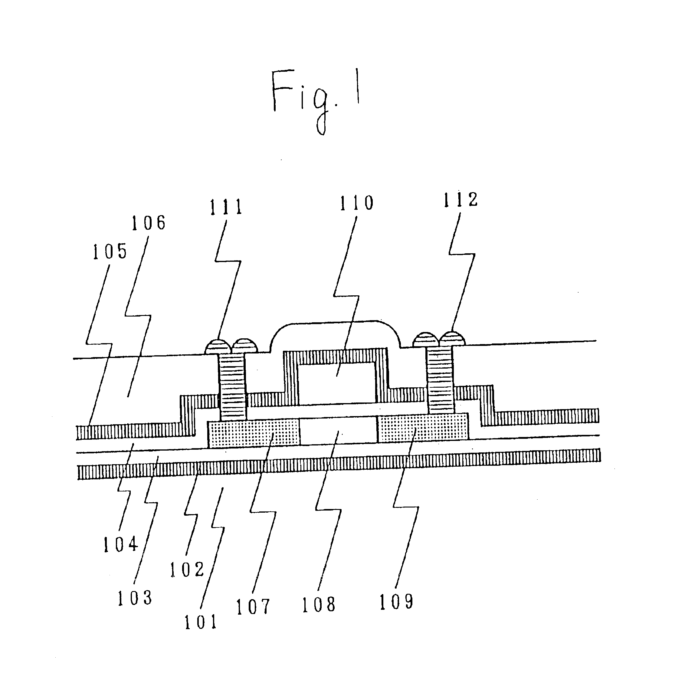
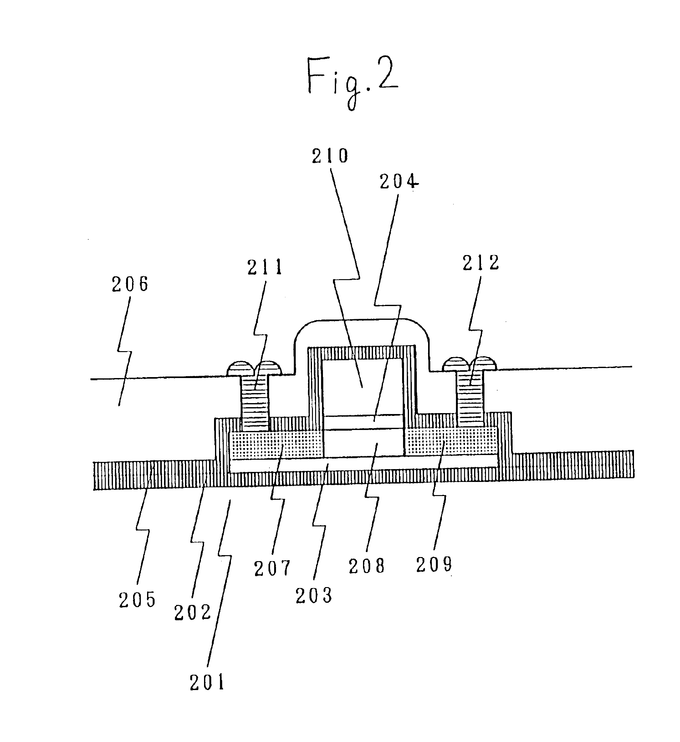
The characteristics of TFT in accordance with the present invention is described as follows. TFT used in this Example was a LDD type TFT prepared on a quartz glass, according to the process of FIG. 4. First of all, a silicon nitride film 402 was formed in 100 nm thick, on a quartz glass 401 and also a back and a side thereof (i.e. in whole surface of the substrate), using a low pressure CVD method. Then, continuously by this low pressure CVD method, a silicon oxide film (insulating film) 403 (a low temperature oxidation film, LTO film) was formed in 200 nm thick. Lastly, by this low pressure CVD method as well, an amorphous silicon film was formed on the silicon oxide film 403 in 30 nm thick. At this time, the maximum process temperature was 600° C.

Next, the amorphous silicon was patterned into the island shape. Then, the very thin surface portion of the amorphous silicon was oxidized, in 2 to 10 nm thick by an anodic oxidation method. The oxidized surface portion comprised...


PUM


Abstract

An improved type thin film semiconductor device and a method for forming the same are described. That is, in a thin film semiconductor device such as TFT formed on an insulating substrate, it is possible to prevent the intrusion of a mobile ion from a substrate or other parts, by forming the first blocking film comprising a silicon nitride, an aluminum oxide, an aluminum nitride, a tantalum oxide, and the like, under the semiconductor device through an insulating film used in a buffering, and then, by forming the second blocking film on TFT, and further, by covering TFT with the first and second blocking films.

Description

BACKGROUND OF THE INVENTION1. Field of the InventionThe present invention relates to a thin film semiconductor device and a method for forming the same. More particularly, the present invention relates to a thin film semiconductor device and a method for forming the same which excel in confidence, productivity, and yield thereof. The present invention is applicable to e.g. a three dimensional integrated circuit or a driving circuit used in a liquid crystal display or a thin film image sensor and the like.2. Description of the Related ArtHeretofore, a semiconductor integrated circuit has been mainly a monolithic type, which has been formed on such semiconductor substrate as silicon. Recently, it has been tried to form it on an insulating substrate made of glass, sapphire, and the like. This is caused by the reasons that an operation speed will be raised according to the lowering of parasitic capacity between a substrate and a wiring, especially quartz or glass materials are not limit...

Claims


Application Information

Patent Timeline
IPC IPC(8): H01L21/02H01L29/786H01L29/66H01L21/336
CPCH01L29/66757H01L29/78603H01L29/78675H01L29/78654H01L29/78621
Inventor YAMAZAKI, SHUNPEITAKEMURA, YASUHIKO
Owner SEMICON ENERGY LAB CO LTD
Why Eureka
Try Eureka