Semiconductor device and fabrication method thereof

a semiconductor film and semiconductor technology, applied in the direction of semiconductor/solid-state device details, instruments, coatings, etc., can solve the problems of affecting the electric characteristics of tft, reducing the mobility of the carrier and the life time, and damage to the crystalline semiconductor film, etc., to achieve high performance and efficient processing

Inactive Publication Date: 2005-02-08
SEMICON ENERGY LAB CO LTD
View PDF14 Cites 31 Cited by
  • Summary
  • Abstract
  • Description
  • Claims
  • Application Information

AI Technical Summary

Benefits of technology

The present invention is directed to provide a high performance semiconductor device that can solve the problems described above, and can be efficiently processed by a hydrogenation process without imparting damage and contamination of a crystalline semiconductor film, and a method of fabricating such a semiconductor device.
A method of fabricating a semiconductor device according to the present invention comprises the steps of forming a hydrogen-containing first insulating film over a semiconductor layer that is formed into a predetermined shape over a substrate, and then conducting heat-treatment in a hydrogen atmosphere or in an atmosphere containing hydrogen that is formed by generating hydrogen plasma. The first insulating film may be an inter-layer insulating film formed over a gate electrode. When hydrogenation is carried out through this first insulating film, the problems of damage to a semiconductor layer and its contamination can be avoided. Because hydrogen is supplied to the hydrogen-containing first insulating film, hydrogen in this first insulating film diffuses into its lower layer and hydrogenation of the semiconductor layer proceeds.
Another method of fabricating a semiconductor device according to the present invention comprises the steps of forming a hydrogen-containing first insulating film over a semiconductor layer that is formed into a predetermined shape over a substrate, conducting then heat-treatment in a hydrogen atmosphere or in an atmosphere containing hydrogen formed by plasma generation, forming a hydrogen-containing third insulating film on the first insulating film, and conducting heat-treatment in an atmosphere containing hydrogen or nitrogen. When the third insulating film comprises a compact film of a silicon nitride oxide or a silicon nitride film, the quantity of hydrogen dissociating from the first insulating film into the gaseous phase can be reduced and hydrogenation of the semiconductor layer can be attained more reliably.
More preferably, the method of fabricating a semiconductor device comprises the steps of forming a hydrogen-containing first insulating film over a semiconductor layer formed into a predetermined shape over a substrate, conducting then heat-treatment in a hydrogen atmosphere or in an atmosphere containing hydrogen that is formed by plasma generation, forming a second insulating film in contact with the first insulating film, conducting heat-treatment in a hydrogen atmosphere or in an atmosphere containing hydrogen formed by plasma generation, and conducting heat-treatment in an atmosphere containing hydrogen or nitrogen after the hydrogen-containing third insulating film is formed on the second insulating film. According to this construction, hydrogen that is supplied by the step of conducting the heat-treatment in the hydrogen atmosphere or in the atmosphere containing hydrogen formed by plasma generation diffuses into the lower layer, and hydrogenation of the semiconductor layer can be effected reliably.

Problems solved by technology

However, because a large number of defects exist in the crystalline semiconductor film so crystallized, mobility of the carriers and the life time are markedly lowered with the result that electric characteristics of the TFT are adversely affected.
In consequence, there remains the problem that the crystalline semiconductor film is damaged by the ions that are formed simultaneously in the plasma.
If any atmospheric components such as nitrogen and oxygen remain in the atmosphere in the plasma hydrogenation method, these elements, too, are converted to the plasma and contaminate the crystalline semiconductor film.
However, the hydrogen concentration introduced into the film by this method has a distribution such that it progressively decreases from the surface to its inside.
For this reason, it has been difficult to sufficiently hydrogenate the crystalline semiconductor film on the lower layer side.
The heat-treatment process in the hydrogen atmosphere as another method involves the problem that the process time gets unavoidably extended in order to improve the hydrogenation effect.

Method used


Image

  • Semiconductor device and fabrication method thereof
  • Semiconductor device and fabrication method thereof
  • Semiconductor device and fabrication method thereof

Examples


example 1

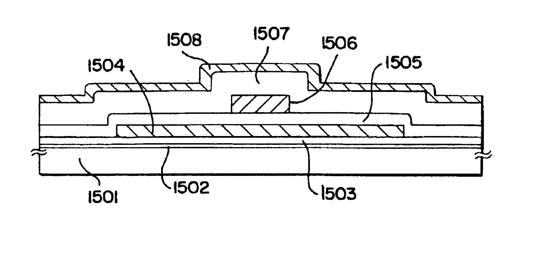
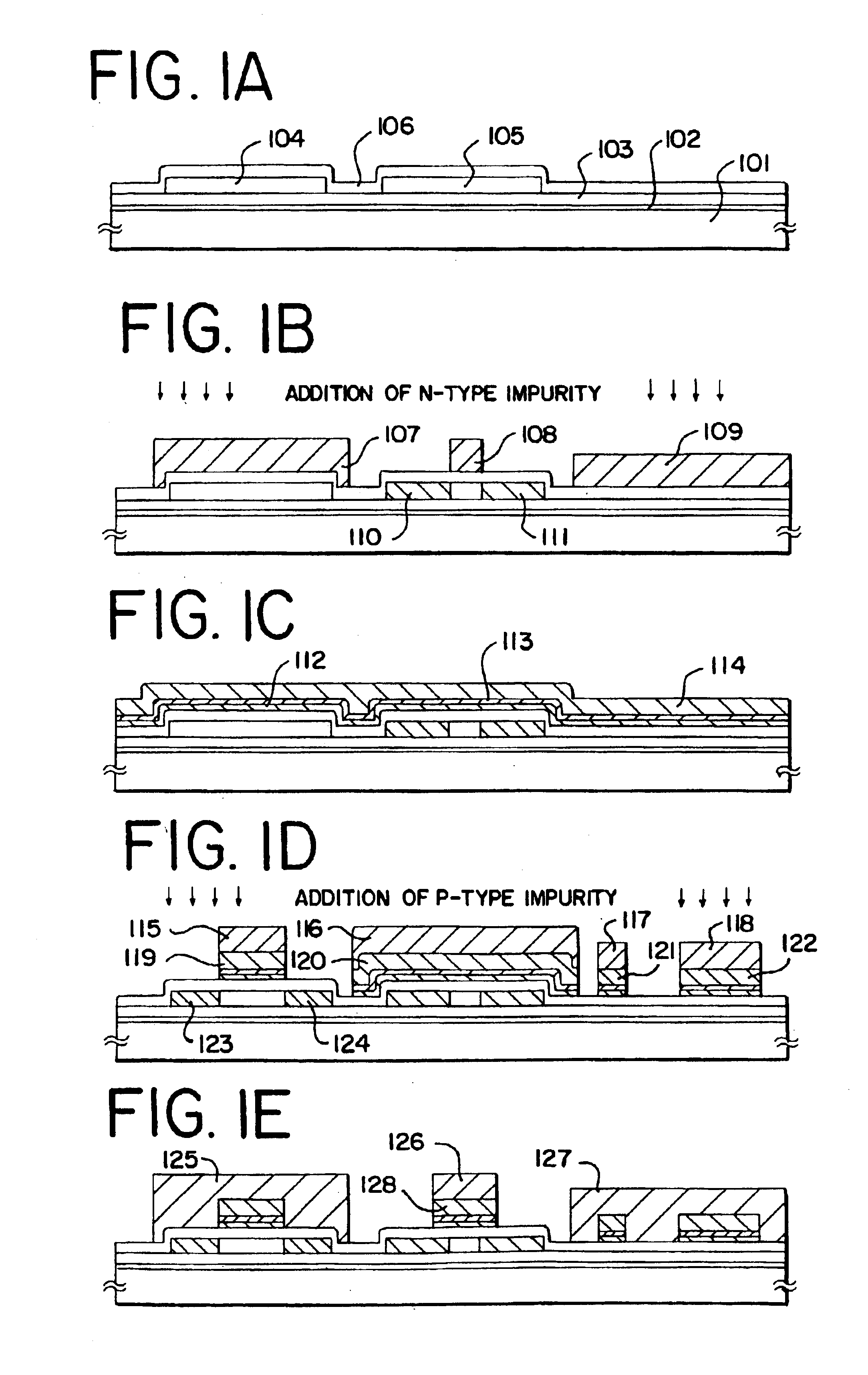
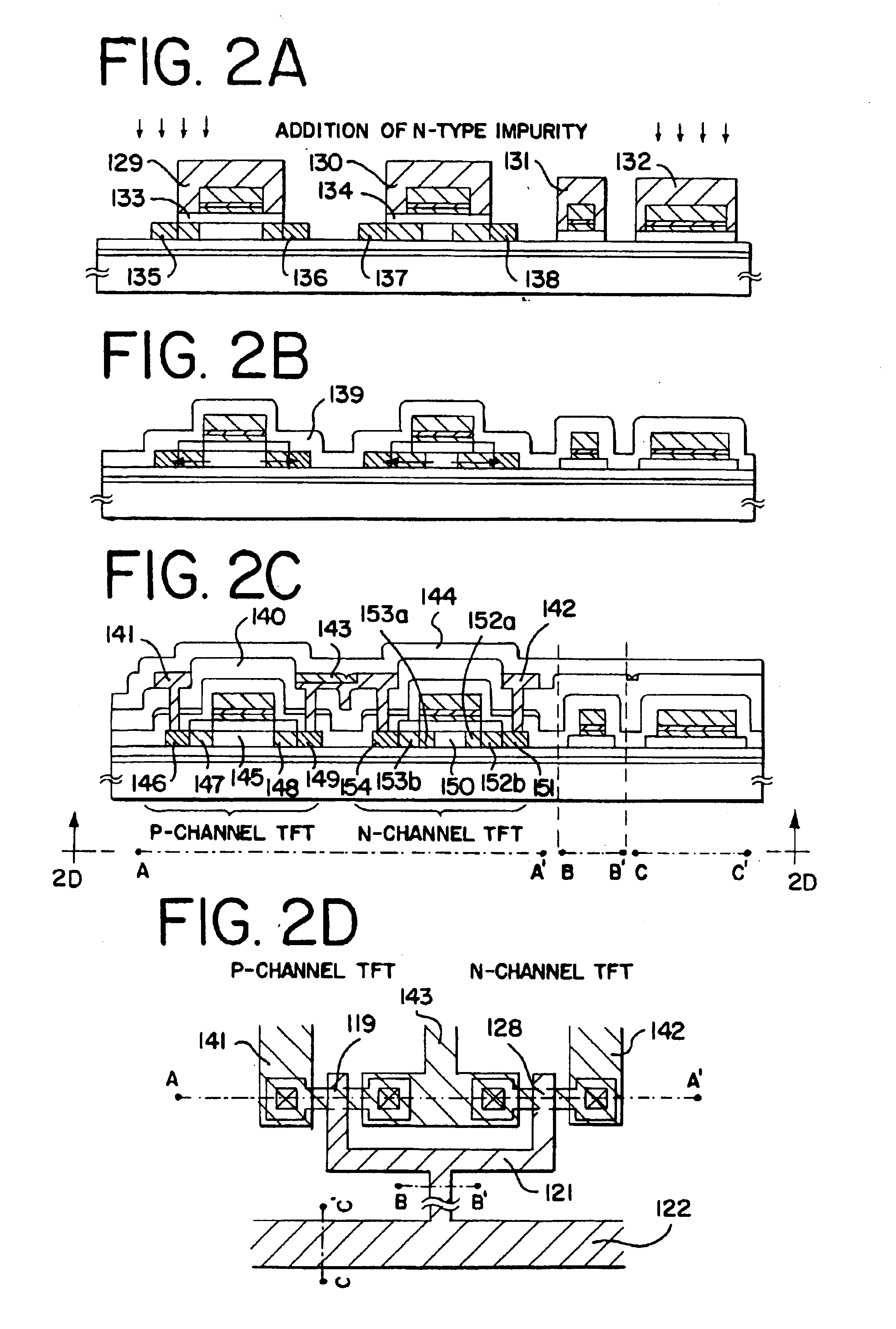
An example of the present invention will be explained in detail about an inverter circuit as the basic construction of a CMOS circuit, by way of example, with reference to FIGS. 1 and 2. Referring to FIG. 1(A), underlying films 102 and 103 are shown formed over a substrate 101 having an insulating surface. The underlying film 102 is a nitrogen-rich silicon nitride oxide film having a nitrogen concentration of at least 25 atomic % to less than 50 atomic %, and its thickness is 20 to 100 nm and typically 50 nm. The underlying film 103 is a silicon nitride oxide film having a nitrogen concentration of at least 5 atomic % to less than 25 atomic %, and its thickness is 50 to 500 nm, typically 150 to 200 nm. A first island-like semiconductor film 105, a second island-like semiconductor film 104 and a gate insulating film 106 are formed over the former. The island-like semiconductor films are acquired by separating into an island shape the crystalline semiconductor film that is in turn for...

example 2

In this example, a method of fabricating an active matrix substrate having a pixel matrix circuit and a CMOS circuit as a basic form of a driving circuit disposed around, and formed simultaneously with, the pixel matrix circuit, will be explained with reference to FIGS. 3 to 5. First, a nitrogen-rich silicon nitride oxide film 302a is formed as a first insulating layer on a substrate 301 to a thickness of 50 to 500 nm, typically to a thickness of 100 nm. A silicon nitride oxide film 302b is formed further to a thickness of 100 to 500 nm, typically to a thickness of 200 nm. The nitrogen-rich silicon nitride oxide film 302a has a nitrogen concentration of at least 25 atomic % to less than 50 atomic %. The silicon nitride oxide film 302b is produced from SiH4, N2O and NH3. Island-like crystalline semiconductor films 303, 304 and 305 and a gate insulating film 306 are further formed. The island-like crystalline semiconductor films are obtained by crystallizing an amorphous semiconductor...

example 3

This example represents an example with reference to FIG. 6 where an active matrix type liquid crystal display device is fabricated from the active matrix substrate produced in Example 2. First of all, an orientation film 401 is formed on a substrate under the state shown in FIG. 5(B). A polyimide resin is used in most cases for the orientation film of the liquid crystal display device. A transparent conductive film 403 and an orientation film 404 are formed on an opposing substrate 402. After being formed, the orientation film is rubbed so that the liquid crystal molecules are arranged in parallel with a predetermined pre-tilt angle. After these steps, the active matrix substrate having the pixel matrix circuit and the CMOS circuit formed thereon and the opposing substrate are bonded to each other through a sealing material and a spacer (both are not shown) by a known cell assembly process. Thereafter, a liquid crystal material 405 is charged between both substrates and is complete...


PUM

PropertyMeasurementUnit
thicknessaaaaaaaaaa
temperatureaaaaaaaaaa

Abstract

A hydrogenation method that utilizes plasma directly exposes a crystalline semiconductor film to the plasma, and therefore involves the problem that the crystalline semiconductor film is damaged by the ions generated simultaneously in the plasma. If a substrate is heated to 400° C. or above to recover this damage, hydrogen is re-emitted from the crystalline semiconductor film.To solve these problems, a method of fabricating a semiconductor device according to the present invention comprises the steps of forming a hydrogen-containing first insulating film on a semiconductor layer formed into a predetermined shape, conducting heat-treatment in a hydrogen atmosphere or in an atmosphere containing hydrogen formed by plasma generation, forming a second insulating film in contact with the first insulating film, conducting heat-treatment in a hydrogen atmosphere or in an atmosphere containing hydrogen formed by plasma generation, forming a hydrogen-containing third insulating film on the second insulating film and conducting heat-treatment in an atmosphere containing hydrogen or nitrogen.

Description

BACKGROUND OF THE INVENTION1. Field of the InventionThis invention relates to a semiconductor device having an active circuit constituted by thin film transistors formed over a substrate, and a method of fabricating the semiconductor device. More particularly, this invention can be used appropriately for fabricating thin film transistors using a crystalline semiconductor layer. The present invention can be utilized also for fabricating an integrated circuit that comprises thin film transistors, an electro-optical device typified by an active matrix display device, and an image sensor, and an electronic appliance having the electro-optical device mounted thereto.2. Description of the Related ArtA semiconductor device typified by an active matrix liquid crystal display device comprising a large number of thin film transistors (TFTs) arranged on a substrate has been developed. In order to accomplish high mobility in the TFTs, it has been believed preferable to use a crystalline semicon...

Claims


Application Information

Patent Timeline
Patent Type & Authority Patents(United States)
IPC IPC(8): H01L21/70H01L21/02H01L21/30H01L29/786H01L29/66H01L21/336H01L27/12H01L21/314H01L21/84H01L21/77H01L29/423H01L29/49
CPCG02F1/1362H01L21/3003H01L21/3144H01L21/3145H01L29/42384H01L29/4908H01L29/66757H01L29/66765H01L29/78621H01L29/78627H01L27/1214G02F1/133345G02F1/13454H01L2029/7863H01L27/124H01L27/127H01L21/02274H01L21/0214H01L21/022H01L21/02211H01L21/0217H01L21/02337
Inventor YAMAZAKI, SHUNPEIASAMI, TAKETOMIKITAKADO, HIDEHITOARAI, YASUYUKI
Owner SEMICON ENERGY LAB CO LTD
Why Eureka
Try Eureka